Method for manufacturing busbar circuit board with thick conductor layer

A manufacturing method and conductor layer technology, which are applied in printed circuit manufacturing, printed circuits, printed circuits, etc., can solve the problems of poor bonding force between the busbar and the insulating layer, high production cost, serious etching side etching effect, etc. The effect of planarization, simple and compact structure, and reduced installation cost

Active Publication Date: 2017-07-14
深圳市牧泰莱电路技术有限公司
View PDF5 Cites 4 Cited by
  • Summary
  • Abstract
  • Description
  • Claims
  • Application Information

AI Technical Summary

Problems solved by technology

[0006] The object of the present invention is to provide a method for making a busbar circuit board with a thick conductor layer, which is used to solve the problem that the busbar in the prior art does not have the function of installing a circuit board. When using a thick conductor layer as a busbar, the busbar and The technical problems of high production cost and complex process are caused by poor bonding force between insulating layers, serious etching side erosion effect, and difficulty in forming busbar lines.

Method used


Image

  • Method for manufacturing busbar circuit board with thick conductor layer
  • Method for manufacturing busbar circuit board with thick conductor layer
  • Method for manufacturing busbar circuit board with thick conductor layer

Examples


Embodiment Construction

[0035] In order to make the technical problems to be solved, technical solutions and advantages of the present invention clearer, the present invention will be further described in detail below in conjunction with the accompanying drawings and embodiments. It should be understood that the specific embodiments described here are only used to explain the present invention, not to limit the present invention.

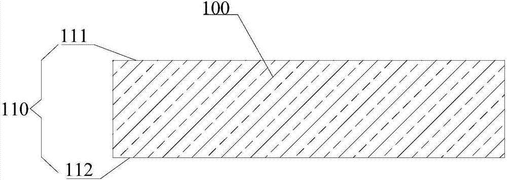
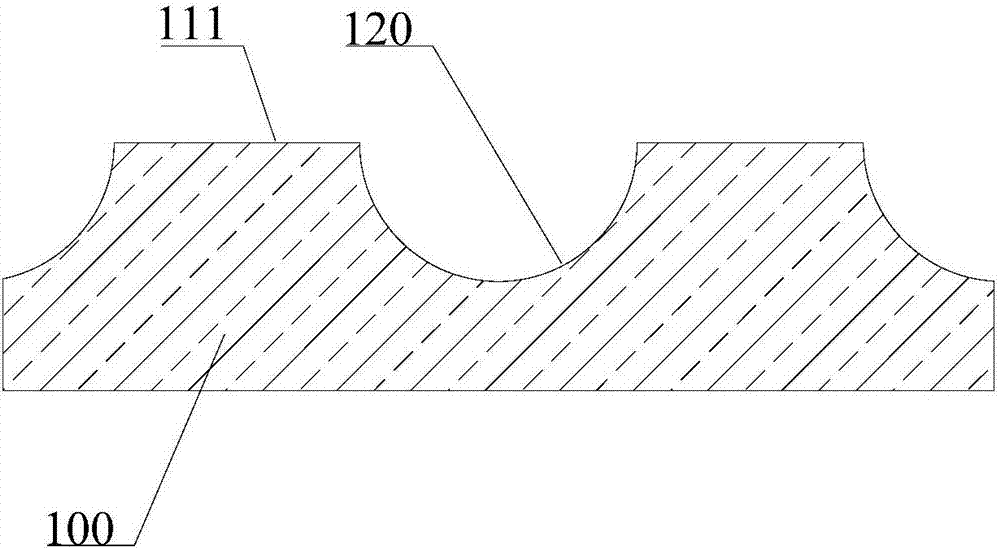
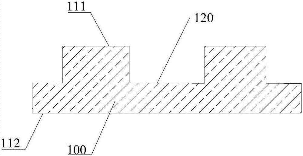
[0036]It should be noted that the same or similar symbols in the drawings of the embodiments of the present invention correspond to the same or similar components; in the description of the present invention, it should be understood ", "right" and other indicated orientations or positional relationships are based on the orientations or positional relationships shown in the drawings, and are only for the convenience of describing the present invention and simplifying the description, rather than indicating or implying that the referred device or element must have a specific ...


PUM


Abstract

The invention belongs to the technical field of busbar manufacturing, and aims to provide a method for manufacturing a busbar circuit board with a thick conductor layer. In the invention, depth-controlled etching and depth-controlled edge milling are respectively performed on a first processing surface and a second processing surface which are oppositely arranged in a conductor layer with required thickness for one time, an insulation bonding layer is laminated to the conductor layer respectively from the first processing surface and the second processing surface so as to process a required busbar, the conductor layer with required thickness is arranged inside a circuit board through combined actions of a series of traditional circuit board manufacturing methods, and the busbar is enabled to have functions of an installation circuit board. In addition, the mode of depth-controlled edge milling is adopted, so that the roughness of the side wall of the conductor layer is increased to a certain degree, thus a binding force between the insulation bonding layer and the conductor layer is ensured, occurrence of undesirable phenomena of board explosion and delamination is reduced as far as possible, and thus manufacturing of a busbar circuit board which is low in production cost, universal and simple in manufacturing process and capable of passing high current can be ensured.

Description

technical field [0001] The invention belongs to the technical field of busbar manufacturing, and more specifically relates to a method for manufacturing a busbar circuit board with a thick conductor layer. Background technique [0002] The so-called busbar is a high-current conductive product used in the power supply system, and its function is basically the same as that of the cable. In the prior art, busbars generally do not have the function of installing circuit boards, and traditional busbars use their metal conductor layers such as copper plates or aluminum plates to connect with other electrical devices. Usually, this wiring method is more complicated and error-prone, not only that , The traditional wiring structure between the busbar and the electrical device occupies a large space and the wiring is relatively complicated. In addition, in order to facilitate the connection of electrical components, traditional busbars are generally processed by mold punching, and ea...

Claims


Application Information

Patent Timeline
Patent Type & Authority Applications(China)
IPC IPC(8): H05K3/00H05K3/42
CPCH05K3/0044H05K3/425H05K2201/09563H05K2203/0214
Inventor 彭湘钟岳松黄文
Owner 深圳市牧泰莱电路技术有限公司
Why Eureka
Try Eureka