


Quick Research
Generate reliable direction feasibility study reports for your R&D in just a few steps.

Technical Q&A
Discover and master advanced knowledge NOW. Basics, ideas, possibilities, all at once.

Find Solutions
As an expert in R&D theories, this can generate solutions to your technical problems instantly.

Evaluate Feasibility
Analyze your overall solution with one click, know your potential R&D risks in advance.

Monitor Landscape
Get weekly tech updates, stay abreast of the latest tech innovations and key insights.
wafer level package led
A technology of wafer-level packaging and LED chips, which is applied in the direction of semiconductor devices, electrical components, circuits, etc., can solve the problems of inability to meet the requirements of directional illumination application scenarios, asymmetric light distribution, and easy short-circuiting of welding to meet the requirements of directional lighting. The effect of sexual exposure application scene requirements
- Summary
- Abstract
- Description
- Claims
- Application Information
AI Technical Summary
Problems solved by technology
Method used
Image

Examples
Embodiment 1
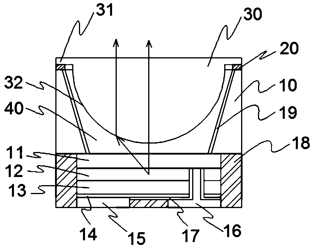
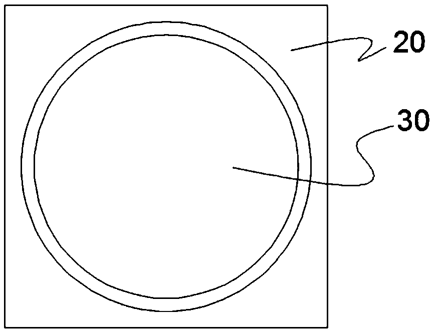
[0022] see figure 1 and 3 The embodiment of the present invention includes an LED chip, a lens 30, and a lens bonding layer 20. The LED chip includes a substrate layer 10 made of GaAs, a first doped semiconductor layer 11 made of AlGaAs, and a semiconductor light-emitting layer made of AlGaAs. 12. The second doped semiconductor layer 13 made of AlGaAs, the conductive reflective layer 14 made of silver, the first electrode 16, the second electrode 15, the insulating layer 17 and the coating medium 18, the semiconductor light-emitting layer 12 is arranged on the Between the first doped semiconductor layer 11 and the second doped semiconductor layer 13 , the conductive light-reflecting layer 14 is disposed under the second doped semiconductor layer 13 , and the second electrode 15 is connected to the second doped semiconductor layer through the conductive light-reflecting layer 14 . 13, the first electrode 16 is directly connected to the first doped semiconductor layer 11 to ach...
Embodiment 2
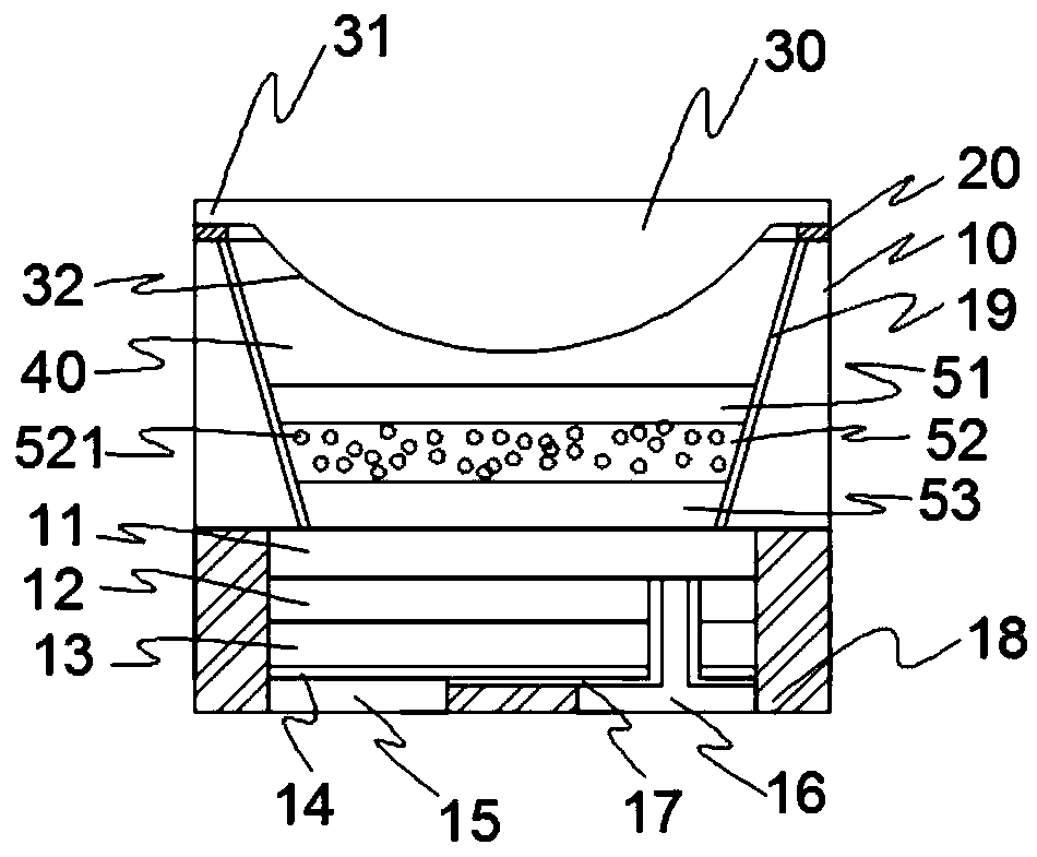
[0030] see figure 2 and 3, a wafer-level packaged LED, comprising an LED chip, a lens 30, and a lens bonding layer 20, the LED chip includes a substrate layer 10 made of silicon, a first doped semiconductor layer 11 made of GaN, and a material of InGaN The semiconductor light-emitting layer 12, the second doped semiconductor layer 13 made of GaN, the conductive reflective layer 14 made of silver, the first electrode 16, the second electrode 15, the insulating layer 17 and the cladding medium 18, the semiconductor light-emitting The layer 12 is arranged between the first doped semiconductor layer 11 and the second doped semiconductor layer 13 , the conductive reflective layer 14 is arranged under the second doped semiconductor layer 13 , and the second electrode 15 is connected to the second doped semiconductor layer 14 through the conductive reflective layer 14 . The electrical conduction between the doped semiconductor layers 13, the first electrode 16 is directly connected...
Embodiment 3
[0041] see figure 2 and 3 , a wafer-level packaged LED, comprising an LED chip, a lens 30, and a lens bonding layer 20. The LED chip includes a substrate layer 10 made of GaAs, a first doped semiconductor layer 11 made of AlGaInP, and a material of AlGaInP. The semiconductor light-emitting layer 12, the second doped semiconductor layer 13 made of AlGaInP, the conductive reflective layer 14 made of Al, the first electrode 16, the second electrode 15, the insulating layer 17 and the coating medium 18, the semiconductor light-emitting The layer 12 is arranged between the first doped semiconductor layer 11 and the second doped semiconductor layer 13 , the conductive reflective layer 14 is arranged under the second doped semiconductor layer 13 , and the second electrode 15 is connected to the second doped semiconductor layer 14 through the conductive reflective layer 14 . The electrical conduction between the doped semiconductor layers 13, the first electrode 16 is directly conne...
PUM
 Abstract
Description
Claims
Application Information
 - R&D Engineer
- R&D Manager
- IP Professional
- Industry Leading Data Capabilities
- Powerful AI technology
- Patent DNA Extraction
Browse by: Latest US Patents, China's latest patents, Technical Efficacy Thesaurus, Application Domain, Technology Topic, Popular Technical Reports.
© 2024 PatSnap. All rights reserved.Legal|Privacy policy|Modern Slavery Act Transparency Statement|Sitemap|About US| Contact US: help@patsnap.com