
Device and method for high-throughput electrochemical characterization of composite material chip

A combined material chip, high-throughput technology, applied in the direction of measuring devices, analytical materials, scientific instruments, etc., can solve the problem that the electrochemical characterization method cannot meet the high-throughput screening requirements of the combined material chip, and achieve a flexible number of probes Changeable, real-time monitoring, and easy-to-achieve effects of the preparation process

Inactive Publication Date: 2017-05-31
UNIV OF SCI & TECH BEIJING
View PDF5 Cites 18 Cited by
  • Summary
  • Abstract
  • Description
  • Claims
  • Application Information

AI Technical Summary

Problems solved by technology

With the unremitting efforts of researchers in recent years, the preparation technology of combined material chips has become increasingly mature, but the existing electrochemical characterization methods cannot meet the high-throughput screening requirements of combined material chips, which has become a major obstacle restricting the development of material genomes. Therefore, developing a set of research methods for rapid characterization of electrochemical performance is a key issue that needs to be solved urgently.

Method used


Image

  • Device and method for high-throughput electrochemical characterization of composite material chip
  • Device and method for high-throughput electrochemical characterization of composite material chip
  • Device and method for high-throughput electrochemical characterization of composite material chip

Examples


Embodiment 1

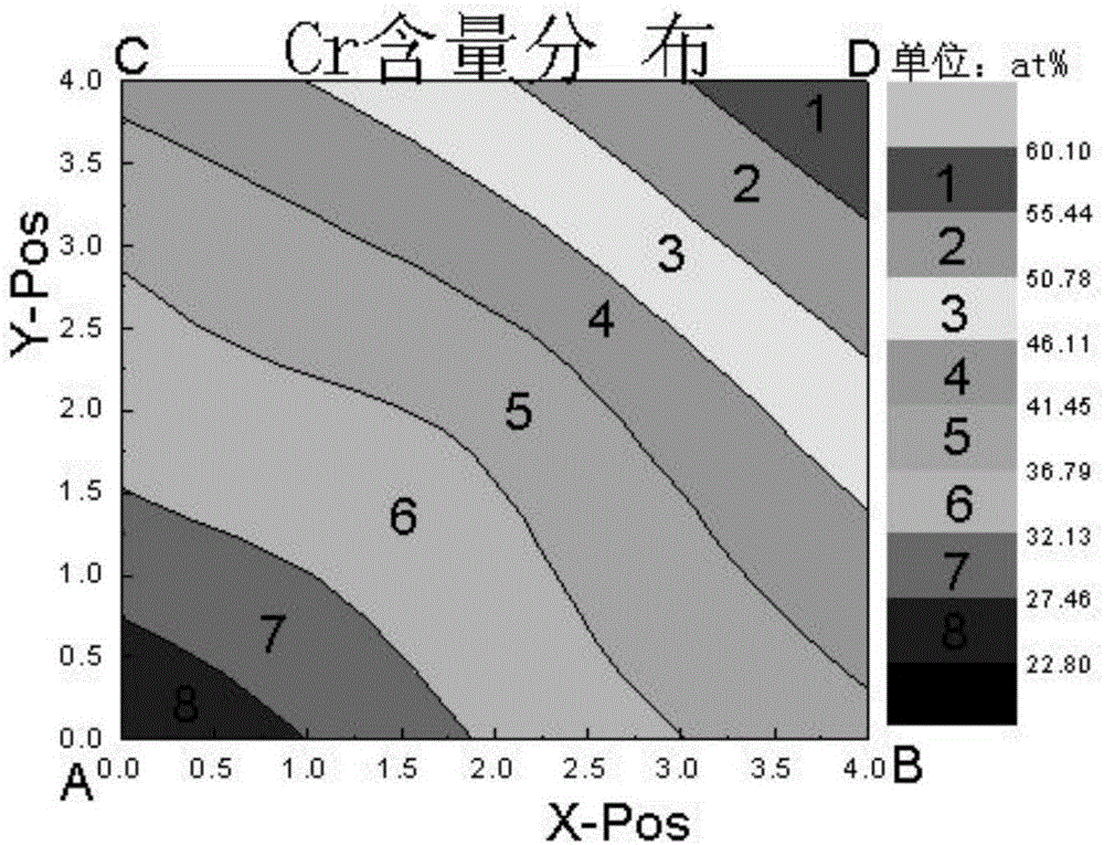
[0026] 304 stainless steel was selected as the substrate for preparing thin film samples, and the substrate size was 40402 mm. A layer of thin film with composition gradient was prepared on the sample by magnetron co-sputtering method, and then the sample was sealed and connected with wires except for the thin film surface to make electrodes. The thin film sample is used as the working electrode, and the wire bundle electrode is used as the auxiliary electrode and reference electrode, and 100 microprobes on the wire bundle electrode are used to measure the current potential distribution in different regions of the thin film sample, and finally the optimal resistance performance components in the composite material chip are obtained Compare. Concretely include the following steps and process conditions:

[0027] (1) Surface pretreatment of stainless steel substrate: Use 400, 800, 1200, 5000 mesh SiC sandpaper to polish the substrate in turn, and then polish until the surface is...

Embodiment 2

[0034] Example 2 The method of preparing a composition gradient film on the surface of stainless steel is basically the same as that of Example 1, except that in step (2) the sputtering angle of copper and chromium is 45°, the sputtering angle of copper is 0, and the sputtering angle of chromium is 0. When the angle is 45 and other conditions remain unchanged, a thin film with a gradient distribution of components is prepared, and a different composition ratio from Example 1 is obtained.


PUM

PropertyMeasurementUnit
diameteraaaaaaaaaa

Abstract

The invention relates to a device and a method for high-throughput electrochemical characterization of a composite material chip. A testing instrument comprises a wire beam electrode, a wire beam electrode current and potential scanner, a film sample with composition gradient distribution and a specific corrosive medium. An electrode potential and current of each probe of the wire beam electrode are obtained by a wire beam electrode measurement method in the wire beam electrode current and potential scanner, so that potential distribution and current distribution in different regions on the surface of the film sample can be compared; finally, local electrochemical parameter information of the surface of the sample to be measured is obtained. The measurement method is simple to operate and can take parallel measurement of the multiple regions at the same time, so that the characterization speed of the electrochemical information can be greatly increased; a quick screening method is provided for corrosion resistance evaluation of a material.

Description

technical field [0001] The invention belongs to the field of electrochemical characterization and corrosion resistance performance detection of thin film materials, and specifically relates to a rapid high-throughput screening method for high-throughput electrochemical characterization of composite material chips that has excellent corrosion resistance performance component ratios in composite material chips Devices and methods. Background technique [0002] At present, the commonly used electrochemical research methods (such as open circuit potential, dynamic potential polarization curve and AC impedance test) are the average signal of the research electrode surface. When the chemical state of the electrode surface is inconsistent, these methods cannot characterize the research electrode surface. Local corrosion, and these research methods use the "fried dish" mode, which can only be tested separately, and the research speed is slow. At present, the country is vigorously d...

Claims


Application Information

Patent Timeline
Patent Type & Authority Applications(China)
IPC IPC(8): G01N17/02
CPCG01N17/02
Inventor 高克玮杨杨宿彦京庞晓露
Owner UNIV OF SCI & TECH BEIJING
Learn More