A method for preparing lead halide perovskite nanowires by recrystallization method
A perovskite and nanowire technology, applied in the direction of titanium halide, nanotechnology, etc., can solve the problems of complex operation, cumbersome process and difficult operation of the two-step method, so as to save the reaction time, improve the light transmission ability and simple operation. Effect
- Summary
- Abstract
- Description
- Claims
- Application Information
AI Technical Summary
Problems solved by technology
Method used
Image
Examples
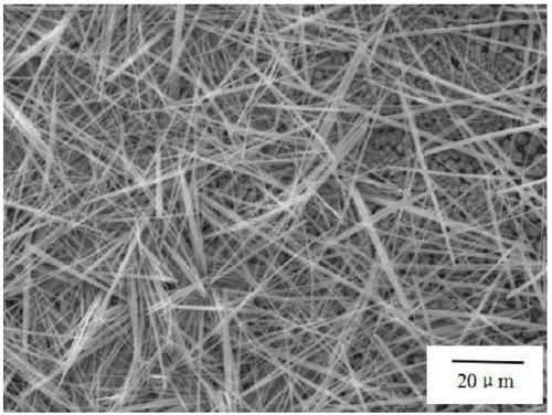
Embodiment 1
[0029] 1) Start ultrasonically cleaning the FTO conductive glass sheet (thickness about 1mm) with detergent for 20 minutes to remove possible organic and inorganic stains on the surface; then rinse with a large amount of tap water; finally put FTO in deionized water Ultrasonic cleaning for 20 minutes; put the above-mentioned cleaned FTO conductive glass into absolute ethanol and ultrasonically clean it for about 20 minutes to remove residual organic impurities on the surface. Repeat this step several times; then ultrasonically clean the FTO conductive glass in acetone for about 20 minutes. For 20 minutes, further remove the residual organic impurities on the surface; take the FTO substrate from the acetone, place it in a UV ozone cleaning machine, and clean it for 30 minutes; the bottom electrode material is SnO doped with fluorine 2 Transparent conductive glass (SnO 2 : F), referred to as FTO.
[0030] 2) Configure 1mol / L CH 3 NH 3 PB 3 The perovskite precursor solution w...
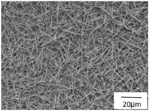
Embodiment 2
[0034] 1) Start ultrasonically cleaning the FTO conductive glass sheet (thickness about 1mm) with detergent for 20 minutes to remove possible organic and inorganic stains on the surface; then rinse with a large amount of tap water; finally put FTO in deionized water Ultrasonic cleaning for 20 minutes; put the above-mentioned cleaned FTO conductive glass into absolute ethanol and ultrasonically clean it for about 20 minutes to remove residual organic impurities on the surface. Repeat this step several times; then ultrasonically clean the FTO conductive glass in acetone for about 20 minutes. For 20 minutes, further remove the residual organic impurities on the surface; take the FTO substrate from the acetone, place it in a UV ozone cleaning machine, and clean it for 30 minutes; the bottom electrode material is SnO doped with fluorine 2 Transparent conductive glass (SnO 2 : F), referred to as FTO.
[0035] 2) Configure 1mol / L CH 3 NH 3 PB 3 The perovskite precursor solution w...
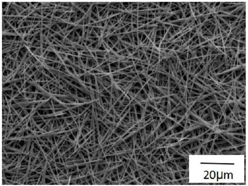
Embodiment 3
[0039] 1) Start ultrasonically cleaning the FTO conductive glass sheet (thickness about 1mm) with detergent for 20 minutes to remove possible organic and inorganic stains on the surface; then rinse with a large amount of tap water; finally put FTO in deionized water Ultrasonic cleaning for 20 minutes; put the above-mentioned cleaned FTO conductive glass into absolute ethanol and ultrasonically clean it for about 20 minutes to remove residual organic impurities on the surface. Repeat this step several times; then ultrasonically clean the FTO conductive glass in acetone for about 20 minutes. For 20 minutes, further remove the residual organic impurities on the surface; take the FTO substrate from the acetone, place it in a UV ozone cleaning machine, and clean it for 30 minutes; the bottom electrode material is SnO doped with fluorine 2 Transparent conductive glass (SnO 2 : F), referred to as FTO.
[0040] 2) Configure 1mol / L CH 3 NH 3 PB 3 The perovskite precursor solution w...
PUM
| Property | Measurement | Unit |
|---|---|---|
| thickness | aaaaa | aaaaa |
Abstract
Description
Claims
Application Information
 - R&D
- Intellectual Property
- Life Sciences
- Materials
- Tech Scout
- Unparalleled Data Quality
- Higher Quality Content
- 60% Fewer Hallucinations
Browse by: Latest US Patents, China's latest patents, Technical Efficacy Thesaurus, Application Domain, Technology Topic, Popular Technical Reports.
© 2025 PatSnap. All rights reserved.Legal|Privacy policy|Modern Slavery Act Transparency Statement|Sitemap|About US| Contact US: help@patsnap.com


