Semiconductor device and manufacturing method thereof, and electronic device
A manufacturing method and semiconductor technology, which are applied to semiconductor devices, electric solid-state devices, radiation control devices, etc., can solve the problems of corrosion, device damage, yield rate, etc., and achieve the effect of reducing cost and improving yield rate.
- Summary
- Abstract
- Description
- Claims
- Application Information
AI Technical Summary
Problems solved by technology
Method used
Image

Examples
Embodiment 1
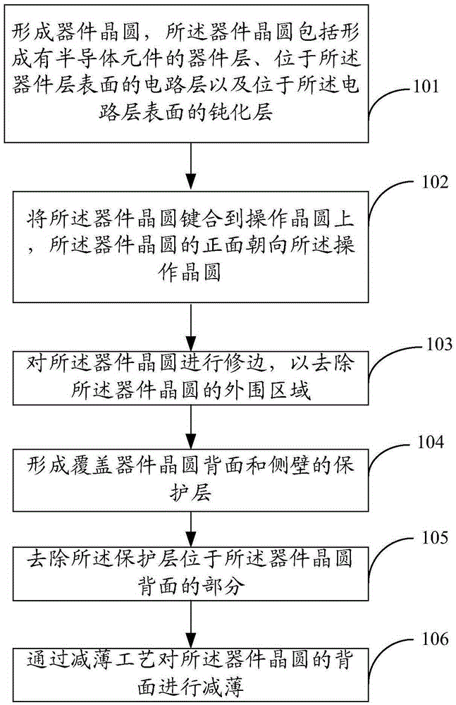
[0035] The following will refer tofigure 1 as well as Figure 2A ~ Figure 2H A method for fabricating a semiconductor device according to an embodiment of the present invention will be described in detail.
[0036] First, step 101 is performed to form a device wafer, the device wafer includes a device layer formed with semiconductor elements, a circuit layer located on the surface of the device layer, and a passivation layer located on the surface of the circuit layer.
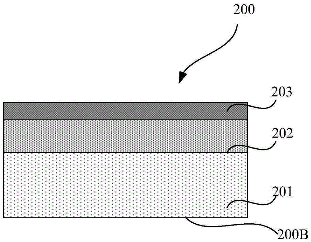
[0037] Such as Figure 2A As shown, a device wafer 200 is formed. The device wafer 200 is a wafer that needs to be thinned, including a device layer 201 formed with semiconductor elements, a circuit layer 202 on the surface of the device, and a passivation layer 203 on the surface of the circuit layer.
[0038] In this embodiment, the device layer 201 is used as a light-transmitting substrate, which may be at least one of the materials mentioned below: Si, Ge, SiGe, SiC, SiGeC, InAs, GaAs, InP or other III ...
Embodiment 2
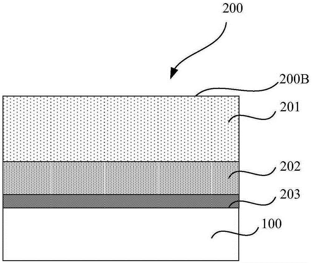
[0070] The present invention also provides a semiconductor device manufactured by the method described in Embodiment 1, such as image 3 As shown, it includes: a device wafer 300, the device wafer 300 includes a device layer 301 formed with semiconductor elements, a circuit layer 302 located below the device, and a passivation layer 303 located below the circuit layer; Operating the wafer 100, the device wafer 300 is bonded to the device wafer 100 through the passivation layer 303, and the surface of the device wafer 300 that is not bonded to the operating wafer 100 is the back side ; and a protective layer 304 covering the sidewall of the circuit layer 302 .
[0071] The device layer 301 is used as a light-transmitting substrate, which may be at least one of the materials mentioned below: Si, Ge, SiGe, SiC, SiGeC, InAs, GaAs, InP or other III / V compound semiconductors, It also includes multi-layer structures composed of these semiconductors, or silicon-on-insulator (SOI), si...
Embodiment 3
[0078] The present invention further provides an electronic device including the aforementioned semiconductor device.
[0079] The electronic device also has the above-mentioned advantages due to the higher performance of the included semiconductor devices.
[0080] The electronic device can be any electronic product or equipment such as mobile phone, tablet computer, notebook computer, netbook, game console, TV, VCD, DVD, navigator, camera, video recorder, voice recorder, MP3, MP4, PSP, etc. It is an intermediate product with the above-mentioned semiconductor device, for example: a mobile phone motherboard with the integrated circuit, etc.
PUM
 Abstract
Description
Claims
Application Information
 - R&D
- Intellectual Property
- Life Sciences
- Materials
- Tech Scout
- Unparalleled Data Quality
- Higher Quality Content
- 60% Fewer Hallucinations
Browse by: Latest US Patents, China's latest patents, Technical Efficacy Thesaurus, Application Domain, Technology Topic, Popular Technical Reports.
© 2025 PatSnap. All rights reserved.Legal|Privacy policy|Modern Slavery Act Transparency Statement|Sitemap|About US| Contact US: help@patsnap.com