
A self-aligning mems piezoresistive accelerometer manufacturing method

The technology of an accelerometer and its manufacturing method is applied in directions such as using inertial force for acceleration measurement, manufacturing microstructure devices, and decorative art, and can solve problems such as piezoresistor asymmetry and adverse effects on device performance, so as to improve device performance and improve The effect of device symmetry and error reduction

Active Publication Date: 2018-07-10
NORTH ELECTRON RES INST ANHUI CO LTD
View PDF7 Cites 0 Cited by
  • Summary
  • Abstract
  • Description
  • Claims
  • Application Information

AI Technical Summary

Problems solved by technology

In this manufacturing method, the varistor layer and the movable structure layer are formed by aligning the photolithographic equipment. Due to the influence of the alignment accuracy of the equipment, the asymmetry of the varistor will be caused, which will adversely affect the performance of the device.

Method used


Image

  • A self-aligning mems piezoresistive accelerometer manufacturing method
  • A self-aligning mems piezoresistive accelerometer manufacturing method
  • A self-aligning mems piezoresistive accelerometer manufacturing method

Examples


Embodiment Construction

[0021] The invention provides a method for manufacturing a self-aligned MEMS piezoresistive accelerometer, comprising the following steps:

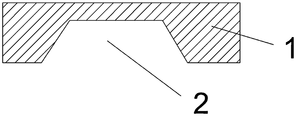
[0022] S1, such as figure 1 As shown, the cavity 2 is fabricated on the bottom surface of the silicon substrate 1 through a KOH etching process;

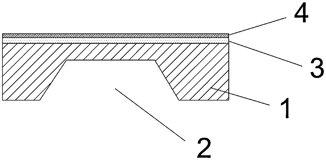
[0023] S2, combine figure 2 As shown, an oxide layer 3 with a thickness of 2000 Å and a silicon nitride layer 4 with a thickness of 2000 Å are grown sequentially from bottom to top on the top surface of the silicon substrate 1 to form a double-layer sacrificial layer;

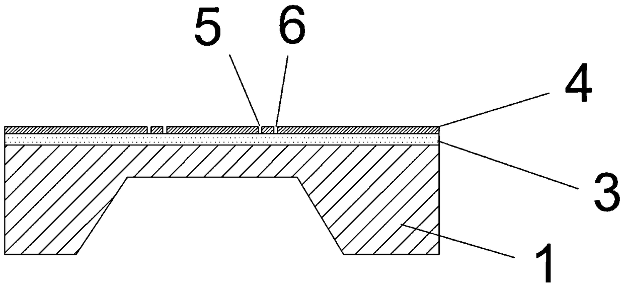
[0024] S3, combine image 3 As shown, on the silicon nitride layer 4, the piezoresistive pattern 5 and the structure release pattern 6 are simultaneously produced by using a photolithography process, and the silicon nitride layer at the piezoresistive pattern and the structure release pattern is etched;

[0025] S4. Combination Figure 4 As shown, the oxide layer 3 at the piezoresistive pattern 5 is etched, and then the pie...


PUM


Abstract

The invention discloses a method of making a self-aligned MEMS piezoresistive accelerometer, comprising the following steps: making a cavity at the bottom of a silicon substrate through a KOH etching process; growing an oxide layer and a silicon nitride layer on the top of the silicon substrate in sequence from bottom to top; making a piezoresistive pattern and a structure release pattern on the silicon nitride layer at the same time through a lithography process, and etching the silicon nitride layer at the piezoresistive pattern and at the structure release pattern; etching the oxide layer at the piezoresistive pattern, and forming a piezoresistor through an injecting process and an annealing process; etching the oxide layer at the structure release pattern to form a structure release area; deeply etching the silicon substrate in the structure release area to form a movable structure, thus getting an MEMS piezoresistive accelerometer. The piezoresistive pattern and the structure release pattern are formed in the same lithography process. There is no need for equipment to carry out alignment in the machining process. Self-alignment of the piezoresistor and a device structure is realized. Thus, the symmetry of devices is improved, error caused by position deviation of the piezoresistor is reduced, and the performance of devices is improved.

Description

technical field [0001] The invention relates to the field of microelectronic machinery, in particular to a method for manufacturing a self-aligned MEMS piezoresistive accelerometer. Background technique [0002] The MEMS piezoresistive accelerometer is a piezoresistor made on a cantilever beam. When the inertial mass moves, it causes the elongation or compression of the cantilever beam, changes the stress distribution on the beam, and then affects the resistance of the piezoresistor. Most of the piezoresistors are located in the most obvious part of the stress change, so that the measurement of acceleration can be realized by forming a Wheatstone bridge through four piezoresistors. [0003] At present, the conventional manufacturing method of MEMS piezoresistive accelerometer is to use photolithography, etching, sputtering and other processes to gradually complete the steps of cavity corrosion, piezoresistor, lead hole, metal lead, and deep structure etching. In this manufa...

Claims


Application Information

Patent Timeline
Patent Type & Authority Patents(China)
IPC IPC(8): B81C1/00G01P15/09G01P15/12
CPCB81C1/00142G01P15/09G01P15/12
Inventor 陈博黄斌王文婧陈璞庄须叶郭群英
Owner NORTH ELECTRON RES INST ANHUI CO LTD
Learn More