Method for realizing enhanced HEMT (high-electron mobility transistor) by using P-type nitride electrochemical etching

An electrochemical and enhanced technology, applied in the field of microelectronics technology, can solve the problems of small etching selection ratio, difficult to control P-type semiconductor etching, etc., and achieve large etching control window, easy mass production, repeatability Good results

Active Publication Date: 2017-03-29
SUZHOU NENGWU ELECTRONICS TECH
View PDF3 Cites 4 Cited by
  • Summary
  • Abstract
  • Description
  • Claims
  • Application Information

AI Technical Summary

Problems solved by technology

But each technology has its own shortcomings
Among them, the P-type cap layer technology does not produce the influence of ion etching on channel electrons, so it has a high saturation current. However, commonly used P-type semiconductors (such as P-AlGaN, P-GaN, P-InGaN, etc.) During dry etching (such as Cl 2 Plasma etching), the barrier layer AlGaN has a small etching selectivity ratio to the P-type semiconductor, so it is difficult to control the complete etching of the P-type semiconductor and stop the etching on the surface of the barrier layer AlGaN

Method used


Image

  • Method for realizing enhanced HEMT (high-electron mobility transistor) by using P-type nitride electrochemical etching
  • Method for realizing enhanced HEMT (high-electron mobility transistor) by using P-type nitride electrochemical etching
  • Method for realizing enhanced HEMT (high-electron mobility transistor) by using P-type nitride electrochemical etching

Examples


Embodiment Construction

[0016] One aspect of the present invention provides a method for realizing enhanced HEMT by electrochemical etching.

[0017] In some embodiments, the method may include:

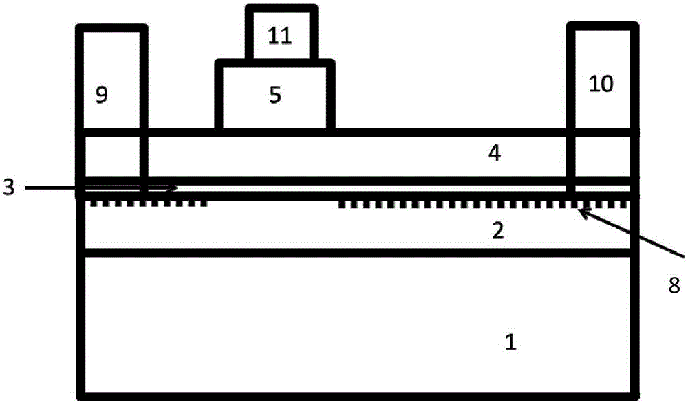
[0018] Provide an etching sample (also referred to as the sample below), the epitaxial structure of the etching sample includes: a heterostructure mainly composed of a first semiconductor layer as a channel layer and a second semiconductor layer as a barrier layer , and, a third semiconductor layer disposed on the second semiconductor layer and depleting the two-dimensional electron gas in the heterostructure conductive channel, and the conductivity of the third semiconductor layer is higher than that of the second semiconductor layer semiconductor layer;

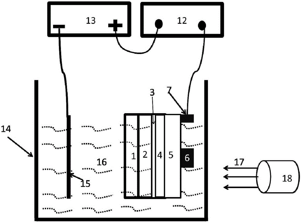
[0019] setting a patterned etching mask on the third semiconductor layer, and directly exposing a region of the third semiconductor layer exposed from the etching mask to an etching solution; The three semiconductor layers provide an etching current wi...


PUM


Abstract

The present invention discloses a method for realizing an enhanced HEMT (high-electron mobility transistor) by using P-type nitride electrochemical etching. The method includes the following steps that: an etching sample is provided, the epitaxial structure of the etching sample comprises a heterostructure and a third semiconductor layer, wherein the heterostructure is composed of a first semiconductor layer and a second semiconductor layer, the third semiconductor layer is arranged on the second semiconductor layer and can deplete a two-dimensional electron gas in the conductive channel of the heterostructure, and the conductivity of the third semiconductor layer is higher than the conductivity of the second semiconductor layer; and a patterned etching mask is arranged on the third semiconductor layer, regions of the third semiconductor layer, which protrude out from the etching mask, are directly exposed in an etching solution, and etching current of a set strength is provided for the third semiconductor layer, and therefore, electrochemical etching on the third semiconductor layer can be realized, and an electrochemical etching process can stop automatically when all regions of the third semiconductor layer except a region covered by the etching mask are completely etched. With the method of the invention adopted, the enhanced HEMT can be effectively realized. The method has the advantages of simple process, etching automatic stop, high repeatability, low cost, small etching loss, easiness in realizing large-scale production and the like.

Description

technical field [0001] The invention discloses a method for preparing a semiconductor device, in particular to a method for realizing an enhanced GaN high electron mobility transistor (HEMT) by electrochemically etching a P-type nitride semiconductor, and belongs to the field of microelectronic technology. Background technique [0002] HEMT devices are made by making full use of the two-dimensional electron gas formed by the heterostructure structure of semiconductors. Compared with the III-VI group (such as AlGaAs / GaAs HEMT), due to the piezoelectric polarization and spontaneous polarization effects of the III-nitride semiconductor, a high concentration of di Dimensional electron gas. Therefore, in HEMT devices made of group III nitrides, the barrier layer generally does not need to be doped. In addition, group III nitrides have the characteristics of large band gap, high saturated electron drift velocity, high critical breakdown electric field and strong radiation resist...

Claims


Application Information

Patent Timeline
IPC IPC(8): H01L29/778H01L21/335
Inventor 张志利张宝顺蔡勇潘革波于国浩付凯孙世闯宋亮秦双娇
Owner SUZHOU NENGWU ELECTRONICS TECH
Why Eureka
Try Eureka