Thin film transistor and manufacturing method and display panel

A technology of thin film transistors and manufacturing methods, applied in the direction of transistors, semiconductor/solid-state device manufacturing, electric solid-state devices, etc., can solve the problem of extending channel length and gate electrode length, deviating from the development trend of high-resolution displays, and enlarging the area of ​​thin-film transistors and other issues, to achieve the effects of reducing parasitic contact resistance, enhancing environmental reliability, and saving manufacturing costs

Inactive Publication Date: 2017-02-22
陆磊 +2
View PDF4 Cites 5 Cited by
  • Summary
  • Abstract
  • Description
  • Claims
  • Application Information

AI Technical Summary

Problems solved by technology

In thin film transistors with traditional back channel etching structure, the exposed upper interface of the channel will be damaged when the electrode is etched, which will affect the performance of the device
Although such damage can be avoided by adding an etch barrier layer on the channel region, this will not only add an additional photolithography process, thereby increasing the manufacturing cost, but more importantly, the device structure of the etch barrier layer needs to extend the trench. The length of the track and the length of the gate electrode will expand the area of ​​the thin film transistor, which will greatly limit the further improvement of the resolution of the display, which deviates from the high-resolution development trend of the display.
In summary, the device structure of back channel etching has the advantages of simple process, lower manufacturing cost and smaller device size, while the device structure of etching barrier layer provides better device performance and Improved device stability, but expands device area and increases manufacturing cost

Method used


Image

  • Thin film transistor and manufacturing method and display panel
  • Thin film transistor and manufacturing method and display panel
  • Thin film transistor and manufacturing method and display panel

Examples


Embodiment Construction

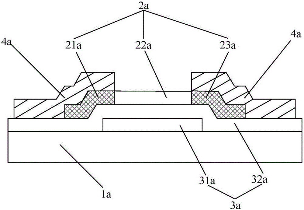
[0039] refer to figure 1 ,figure 1 It is a cross-sectional view of a back gate thin film transistor with a conventional back channel etching structure. Wherein, the thin film transistor includes: a substrate 1a, and an active layer 2a disposed on the substrate 1a. A gate stack 3a is further disposed between the active layer 2a and the substrate 1a. The gate stack 3a includes a gate electrode 31a and a gate insulating layer 32a disposed between the gate electrode 31a and the active layer 2a. The active layer 2a is covered with an electrode 4a. The area where the active layer 2a is in contact with the electrode 4a forms a source area 21a and the drain area 23a respectively, and the area where the active layer 2a is in contact with the non-electrode 4a forms a channel area 22a. Wherein, the channel region 22a is adjacent to the gate stack 3a, and the source region 21a and the drain region 23a are respectively located at two ends of the channel region 22a and connected to the c...


PUM


Abstract

A thin film transistor comprises: a substrate and an active layer made of a metal oxide disposed on said substrate, said active layer being adjacent to a gate stack;the active layer is partially covered with an electrode, and an insulating layer is further included between the electrode and the active layer; wherein the active layer forms a source region and a drain region in a region covered by the electrode, and a region under which the electrode is not covered forms a channel region. The present invention also relates to a thin film transistor manufacturing method and a display panel having the above-described thin film transistor. The thin film transistor described above has both a small size of a conventional back channel etched structure transistor and a superior performance over conventional etching barrier structure transistors, including low source and drain parasitic resistance, better on-state and off-state performance, Enhanced reliability. The display panel with the above-described thin film transistor has the advantages of high performance, high reliability and low cost, and more in line with the development trend of the display panel.

Description

technical field [0001] The invention relates to a metal oxide thin film transistor structure and a manufacturing method thereof, in particular to a thin film transistor structure used in a display panel. Background technique [0002] Conventional metal oxide thin film transistors use metal deposited on the active layer as electrodes. A Schottky barrier is usually formed at the contact interface between the electrode and the active layer, making the resistance of the contact interface very high, thereby increasing the parasitic contact resistance of the thin film transistor, while the intrinsic metal oxide semiconductor is usually High-resistivity, which brings about the problem of high-resistivity source-drain resistance. The existing solution is to reduce the resistivity of the source region and the drain region by doping the source region and the drain region, but this is usually at the cost of sacrificing process stability and increasing manufacturing cost. For example,...

Claims


Application Information

Patent Timeline
Patent Type & Authority Applications(China)
IPC IPC(8): H01L29/786H01L29/10H01L29/08H01L27/12H01L21/324
CPCH01L21/324H01L21/702H01L21/707H01L21/77H01L21/82H01L27/12H01L27/1214H01L27/1225H01L27/1251H01L27/1259H01L29/0603H01L29/0684H01L29/0847H01L29/1033H01L29/66742H01L29/786H01L2021/775H01L21/8236
Inventor 陆磊王文郭海成
Owner 陆磊
Why Eureka
Try Eureka