High-accuracy organic light-emitting device (OLED) component preparation device and method
A preparation device and high-precision technology, applied in the field of OLED, can solve the problems of material waste, difficulty in preparing high-precision OLED devices, mask material and high production requirements, etc., to save evaporation materials, accurately control film thickness, increase effect of number
- Summary
- Abstract
- Description
- Claims
- Application Information
AI Technical Summary
Problems solved by technology
Method used
Image
Examples
preparation example Construction
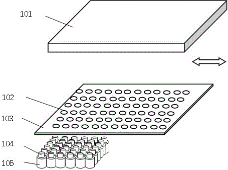
[0028] A preparation device of a high-precision OLED device of the present invention includes an evaporation source array, a substrate, and a transmission device. The evaporation source array is formed by arranging several evaporation sources. The material in the evaporation source is heated to form a molecular flow and evaporates vertically upward to the substrate. The movement of the substrate or the evaporation source array is driven by the transmission device to complete the evaporation of the substrate and form an OLED device.
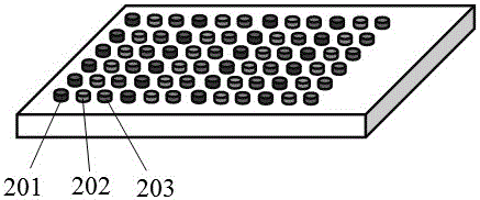
[0029] Each evaporation source in the evaporation source array is equipped with only one sub-pixel evaporation material, three evaporation sources are a basic unit, and the three evaporation sources are respectively placed with red, green and blue sub-pixel evaporation materials, and a basic unit The position of the evaporation source for placing the red, green and blue hair sub-pixel materials in the center is adjustable. Each evaporation source ...
Embodiment 1
[0040] The evaporation of the light-emitting layer of the organic electroluminescent device (OLED) in this embodiment is as follows:
[0041] (1) Processing substrate:
[0042] Use pure water, acetone, ethanol, and pure water to ultrasonically clean the ITO glass for 10-15 minutes each, and then dry the washed ITO glass in an oven or blow dry with nitrogen. Then plasma treatment or UV treatment is performed on the clean and dry substrate.
[0043] (2) Evaporation of luminescent layer:
[0044]Place the above-mentioned ITO glass substrate with anode in a vacuum chamber, the surface of the substrate facing the evaporation source is directly covered with a mask, the area of the substrate is 5cm*5cm; the array of the mask is 96*64, according to the mask The number of combinations of evaporation heads selected for array graphics is 64 in a row, and the diameter of the evaporation heads is 100 μm. The spacing of the evaporation heads depends on the spacing of the 64 sub-pixels i...
Embodiment 2
[0047] The structure adopted by the organic electroluminescence device (OLED) in this embodiment may be:
[0048] Substrate / anode / hole injection layer (HIL) / hole transport layer (HTL) / organic light emitting layer (EML) / electron transport layer (ETL) / electron injection layer (ETL) / cathode.
[0049] Specifically, the structure adopted by the structured organic electroluminescent device in this embodiment is as follows:
[0050] ITO / HAT(CN)6 / NPB / DPVBi / Bphen / LiF / Al
[0051] The preparation method of the organic electroluminescent device of the present embodiment is as follows:
[0052] (1) Processing substrate:
[0053] Clean the ITO glass with pure water, acetone, ethanol, and pure water in sequence, and then dry the washed ITO glass in an oven or blow dry with nitrogen; plasma treatment or UV treatment can be performed on the substrate.
[0054] (2) Evaporation of each functional layer:
[0055] Place the above-mentioned ITO glass substrate with anode in a vacu...
PUM
| Property | Measurement | Unit |
|---|---|---|
| diameter | aaaaa | aaaaa |
Abstract
Description
Claims
Application Information
 - R&D
- Intellectual Property
- Life Sciences
- Materials
- Tech Scout
- Unparalleled Data Quality
- Higher Quality Content
- 60% Fewer Hallucinations
Browse by: Latest US Patents, China's latest patents, Technical Efficacy Thesaurus, Application Domain, Technology Topic, Popular Technical Reports.
© 2025 PatSnap. All rights reserved.Legal|Privacy policy|Modern Slavery Act Transparency Statement|Sitemap|About US| Contact US: help@patsnap.com


