Pi-conjugated organic semiconductor molecular self-assembly structure and preparation method thereof
A molecular and molecular layer technology, applied in the field of monomolecular layer film self-assembly structure, to achieve the effect of improving the efficiency of optoelectronic devices, improving the conversion rate, and good optoelectronic properties
- Summary
- Abstract
- Description
- Claims
- Application Information
AI Technical Summary
Problems solved by technology
Method used
Image
Examples
Embodiment 1
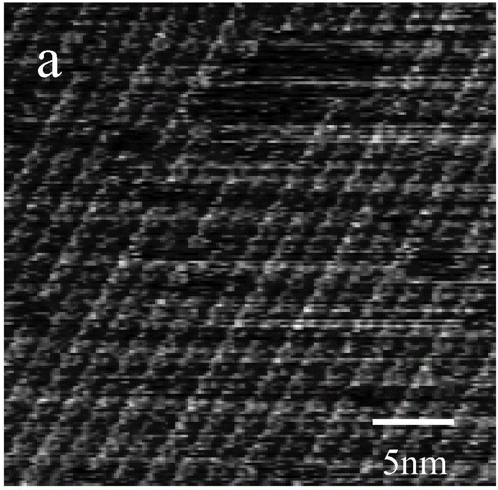
[0049] In a 1.5mL centrifuge tube, add CDI (about 0.5mg) to 1mL of 1-octylbenzene, ultrasonically disperse for about 20 minutes to completely dissolve the molecules, dilute ten times, transfer to the dropper and drop a drop of the solution (about 1μL ) to a clean HOPG surface (newly exfoliated HOPG), since both graphite and the solution are hydrophobic, the solution diffuses on the graphite surface to form a film with uniform thickness, and CDI molecules are adsorbed on the HOPG surface to form a two-dimensional high-density single-layer film nanofilm structure.
[0050] Fix the HOPG dripped with the above solution on the sample stage, and then slowly approach the STM needle tip (Pt / Ir, 80:20) to the sample surface until it is immersed in the solid / liquid interface, but does not touch the graphite surface, and then scan with A tunneling microscope (STM) was used to measure, and the STM image of the ordered CDI between the solid / liquid interface was obtained (refer to Figure 1A...
Embodiment 2
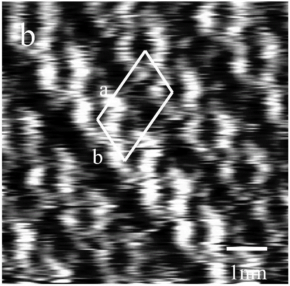
[0055] In a 1.5mL centrifuge tube, add BPMI (about 0.4mg) to 1mL of 1-octylbenzene, ultrasonically disperse for about 20 minutes to completely dissolve the molecules to ensure uniform dispersion, dilute ten times, then transfer to a dropper and drop a drop solution (about 1 μL) onto the clean and flat surface of HOPG. Since both graphite and the solution are hydrophobic, after the solution diffuses on the graphite surface and stabilizes, fix the HOPG dripped with the above solution on the sample stage, and then make the STM needle tip (Pt / Ir, 80:20) slowly approach the sample surface until it is immersed in the solid / liquid interface, but does not touch the graphite surface, scan with a scanning tunneling microscope (STM), and obtain the STM image of the ordered BPMI molecule (reference Figure 2a , Figure 2b ). Depend on Figure 2a and Figure 2b It can be seen that BPMI forms a two-dimensional ordered pore structure.
[0056] refer to Figure 2a and 2b , the brighter...
PUM
 Abstract
Description
Claims
Application Information
 - R&D Engineer
- R&D Manager
- IP Professional
- Industry Leading Data Capabilities
- Powerful AI technology
- Patent DNA Extraction
Browse by: Latest US Patents, China's latest patents, Technical Efficacy Thesaurus, Application Domain, Technology Topic, Popular Technical Reports.
© 2024 PatSnap. All rights reserved.Legal|Privacy policy|Modern Slavery Act Transparency Statement|Sitemap|About US| Contact US: help@patsnap.com


