
Method for preparing solvated nanocrystalline thermoelectric thin film through interface control method

A thermoelectric thin film, nanocrystalline technology, applied in the manufacture/processing of thermoelectric devices, nanotechnology for materials and surface science, nanotechnology, etc. The effect of promoting wide application, improving thermoelectric performance, and wide applicability

Active Publication Date: 2017-01-11
THE NAT CENT FOR NANOSCI & TECH NCNST OF CHINA
View PDF8 Cites 5 Cited by
  • Summary
  • Abstract
  • Description
  • Claims
  • Application Information

AI Technical Summary

Problems solved by technology

[0007] Aiming at the problem that the surface of the existing solvated nanocrystalline film often has long-chain organic ligands, which hinder the transmission of electrons between the nanocrystals and reduce the conductivity of the nanocrystal film, the present invention provides a mild interface regulation Method for preparing solvated nanocrystalline thermoelectric thin film

Method used


Image

  • Method for preparing solvated nanocrystalline thermoelectric thin film through interface control method
  • Method for preparing solvated nanocrystalline thermoelectric thin film through interface control method
  • Method for preparing solvated nanocrystalline thermoelectric thin film through interface control method

Examples


Embodiment 1

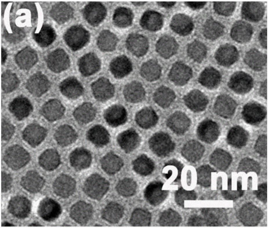
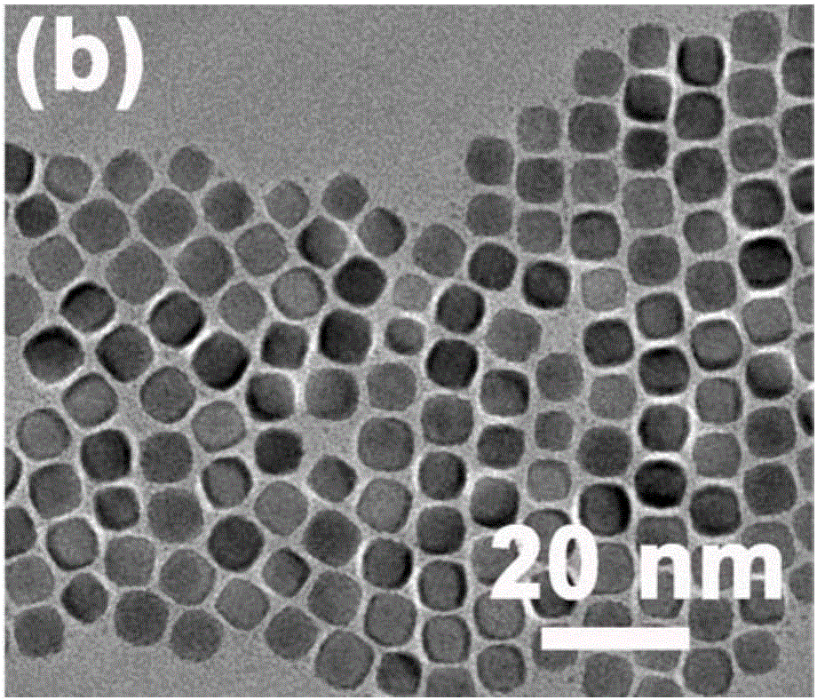
[0101] This embodiment provides a method for wet chemical synthesis of solvated nanocrystals, the method comprising the following steps:

[0102] (1) Preparation of lead telluride (PbTe) nanocrystals:

[0103] Mix 2.5mmol of lead acetate trihydrate, 7.5mmol of oleic acid and 20mL of diphenyl ether evenly, vacuumize and heat at 70°C, and degas at this temperature for 3h. Then nitrogen gas is introduced into the reaction device, and the solution is heated to 180 ° C. At this temperature, 10 mL of TOPTe solution with a concentration of 0.75 M is rapidly injected (in a glove box, tellurium powder is dissolved in n-trioctylphosphine (TOP) solution Middle), the reaction solution was reacted at 155-160° C. for about 2 minutes. The heating was removed and the reactor was cooled to room temperature with a water bath.

[0104] Clean the nanocrystals in the container in an argon glove box, first disperse in 5mL toluene, then precipitate with a mixture of ethanol / acetone, centrifuge at ...

Embodiment 2

[0113] This embodiment provides a method for preparing a solvated PbTe nanocrystalline thermoelectric film by an interface control method, the method comprising the following steps:

[0114] (1) The PbTe nanocrystalline n-octane solution of 10mg / mL prepared in Example 1 is spin-coated on the substrate for 40s at a speed of 1000rpm to obtain a nanocrystalline film coating;

[0115] (2) Soak the nanocrystalline thin film coating prepared in step (1) in a solution of ethylenediamine acetonitrile with a concentration of 0.1mol / L, and react at a constant temperature of 50°C for 30min under an inert environment to carry out ligand removal reaction, and then Rinse with pure acetonitrile solution and dry;

[0116] (3) Anneal the nanocrystalline film stripped of the original ligand in an argon atmosphere, the annealing temperature is 300 ° C, the annealing time is 40 min, repeat the whole preparation process 3 times, and obtain a solvated PbTe with a thickness of about 50 nm Nanocryst...

Embodiment 3

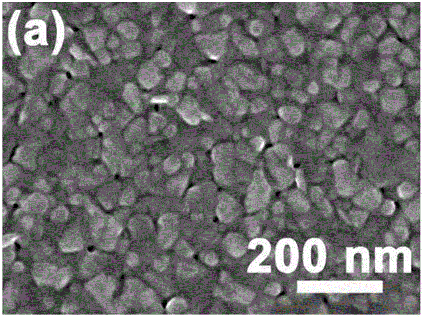
[0119] This embodiment provides a method for preparing solvated PbTe nanocrystalline thermoelectric thin film by interface control method, except that the annealing temperature in step (3) is 350°C, the amount of other materials and the preparation method are the same as those in Example 2 same.

[0120] The thermoelectric properties of the prepared solvated PbTe nanocrystalline thermoelectric thin film are shown in Table 1, and its scanning electron microscope picture is shown in Figure 2(b).


PUM

PropertyMeasurementUnit
thicknessaaaaaaaaaa
thicknessaaaaaaaaaa
particle diameteraaaaaaaaaa

Abstract

The present invention provides a method for preparing a solvated nanocrystalline thermoelectric thin film through an interface control method. The method includes the following the steps that: (1) a solvated nanocrystalline solution is spin-coated on a substrate, so that a nanocrystalline thin film can be prepared; (2) the obtained nanocrystalline thin film is immersed in a short-chain ligand solution, an original organic ligand on the surface of the nanocrystalline thin film is stripped; and (3) annealing treatment is performed on the nanocrystalline thin film of which the original organic ligand is stripped, so that the solvated nanocrystalline thermoelectric thin film can be obtained. The solvated nanocrystalline thermoelectric thin film prepared through the interface control method has excellent thermoelectric performance. The method is compatible with semiconductor device preparation methods in the current microelectronics field and has the advantages of high operability, low cost and wide applicability. With the method adopted, a direction is guided for the large-scale production and preparation of thermoelectric thin film devices in the microelectronics field.

Description

technical field [0001] The invention belongs to the field of nanomaterial preparation, relates to a method for preparing solvated nanocrystal thermoelectric thin film, in particular to a mild method for preparing solvated nanocrystal thermoelectric thin film through an interface control method. Background technique [0002] Thermoelectric materials can realize the conversion of thermal energy and electrical energy, and the thermoelectric performance of the device depends on its quality factor ZT, ZT=(S 2 σT / κ), where S is the Seebeck coefficient, σ is the electrical conductivity, κ is the thermal conductivity, and T is the absolute temperature (M.S.Dresselhaus, G.Chen, M.Y.Tang, R.Yang, H.Lee, D.Wang, Z . Ren, J.P. Fleurial, P. Gogna. Adv. Mater. 2007, 19, 1043). Thermoelectric thin film devices can achieve a lower size, which makes thermoelectric thin film devices more suitable for existing microelectronic packaging technology, and it is also easier to realize fixed-point ...

Claims


Application Information

Patent Timeline
Patent Type & Authority Applications(China)
IPC IPC(8): H01L35/34B82Y30/00H10N10/01
CPCB82Y30/00H10N10/01
Inventor 唐智勇丁德芳
Owner THE NAT CENT FOR NANOSCI & TECH NCNST OF CHINA
Learn More