A T-slot gate mosfet

A trench gate and deep trench technology, applied in the field of power semiconductors, can solve problems such as device threshold and on-resistance, and achieve the effects of preventing failure, increasing gate-source capacitance, and reducing gate-drain capacitance

Inactive Publication Date: 2019-03-29
UNIV OF ELECTRONICS SCI & TECH OF CHINA
View PDF4 Cites 0 Cited by
  • Summary
  • Abstract
  • Description
  • Claims
  • Application Information

AI Technical Summary

Problems solved by technology

However, these methods have an impact on the threshold and on-resistance of the device

Method used


Image

  • A T-slot gate mosfet
  • A T-slot gate mosfet
  • A T-slot gate mosfet

Examples


Embodiment Construction

[0024] The present invention is described in detail below in conjunction with accompanying drawing

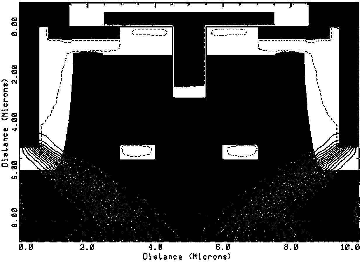
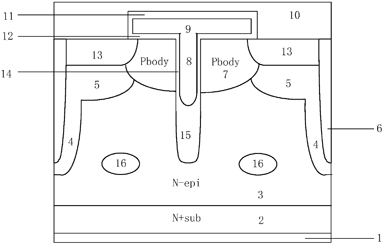
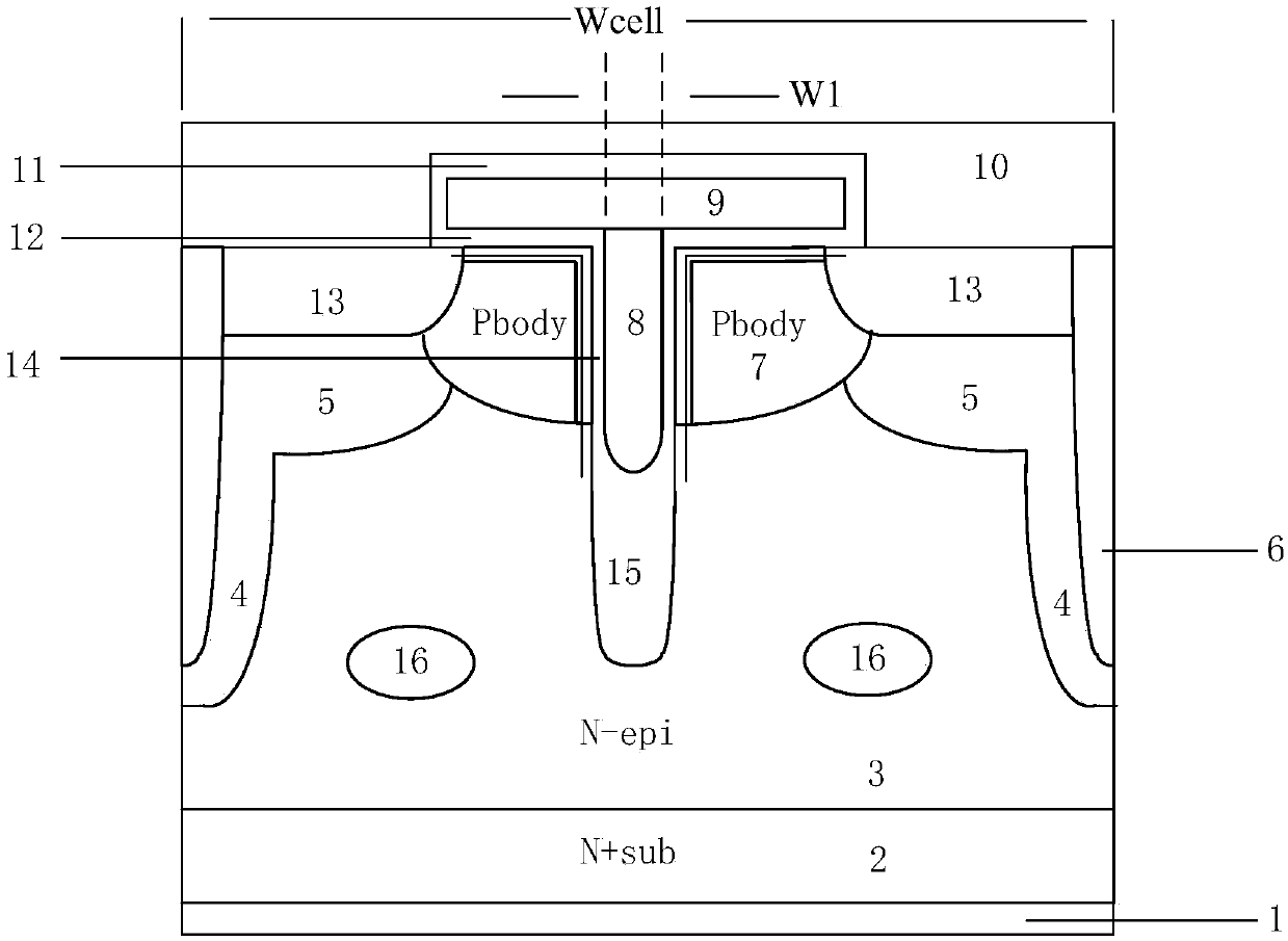
[0025] Such as figure 1 As shown, a T-groove gate MOSFET of the present invention includes a drain electrode 1, an N-type heavily doped single crystal silicon substrate 2, an N-epitaxial layer 3, and a source electrode 10 that are sequentially stacked from bottom to top; The middle part of the upper layer of the N-epitaxial layer 3 has a P body region 7, and both sides of the N-epitaxial layer 3 have deep groove metal 6; the upper surface of the deep groove metal 6 is in contact with the source electrode 10; the P body region 7 The upper layer of the N- epitaxial layer 3 between the deep trench metal 6 has an N+ doped region 13, the upper surface of the N+ doped region 13 is in contact with the source electrode 10, and the sides of the N+ doped region 13 are respectively connected to the P body region 7 is in contact with the deep groove metal 6; there is a P-type base region ...


PUM


Abstract

The invention belongs to the technical field of power semiconductors, in particular to a T-shaped groove gate MOSFET. The invention introduces a T-shaped gate structure, which increases the input capacitance of the device, and the thick oxide layer under the T-shaped gate reduces the Cgd of the device at the same time, so that the ratio of Cgs / Cgd is improved, and the device has higher resistance to drain voltage shocks to the gate Pole impact capability, and low EMI noise. The deep groove metal connection is deeply implanted into the P+ region. This deep groove body contact structure makes it more difficult to turn on the parasitic triode of the device, preventing the UIS thermal failure that is easy to occur during the shutdown process of the device. At the same time, the deeply implanted P+ region and the buried layer p+ The region introduces a transverse electric field, which improves the reverse withstand voltage of the device.

Description

technical field [0001] The invention belongs to the technical field of power semiconductors, in particular to a T-shaped groove gate MOSFET. Background technique [0002] Due to the influence of various parasitic parameters in the drive circuit and the gate capacitance of the power MOS transistor in the high-power drive circuit, the drive signal will oscillate uncertainly, and the gate oscillation will greatly affect the performance and stability of the system. In the device design process, the larger the gate resistance, the smaller the gate oscillation, and the smaller the gate-to-drain capacitance, the smaller the gate oscillation. However, there is a compromise relationship between the EMI characteristics of the power MOS tube and the switching characteristics of the power tube, so it is often necessary to consider various parameters of the device at the same time in the design to obtain the optimal switching characteristics and EMI resistance. Both the currently propos...

Claims


Application Information

Patent Timeline
Patent Type & Authority Patents(China)
IPC IPC(8): H01L29/78H01L29/423H01L29/06
CPCH01L29/0684H01L29/4236H01L29/78
Inventor 李泽宏陈哲曹晓峰李爽陈文梅林育赐谢驰任敏
Owner UNIV OF ELECTRONICS SCI & TECH OF CHINA
Why Eureka
Try Eureka