


Quick Research
Generate reliable direction feasibility study reports for your R&D in just a few steps.

Technical Q&A
Discover and master advanced knowledge NOW. Basics, ideas, possibilities, all at once.

Find Solutions
As an expert in R&D theories, this can generate solutions to your technical problems instantly.

Evaluate Feasibility
Analyze your overall solution with one click, know your potential R&D risks in advance.

Monitor Landscape
Get weekly tech updates, stay abreast of the latest tech innovations and key insights.
An organic light emitting display device and its manufacturing method
A light-emitting display, organic technology, applied in the manufacture of organic light-emitting display devices, the field of organic light-emitting display devices, can solve the problem of not being able to meet the electrical properties at the same time, and achieve the effect of rapid opening and closing
- Summary
- Abstract
- Description
- Claims
- Application Information
AI Technical Summary
Problems solved by technology
Method used
Image


Examples
Embodiment 1
[0041] Figure 4 A schematic cross-sectional structure diagram of an organic light emitting display device according to an embodiment of the invention is shown. Such as Figure 4 As shown, the organic light emitting display device of this embodiment includes a switching thin film field effect transistor T1, a driving thin film field effect transistor T2, and a storage capacitor respectively connected to the switching thin film field effect transistor T1 and the driving thin film field effect transistor T2.
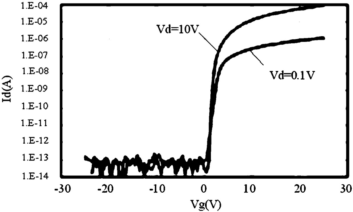
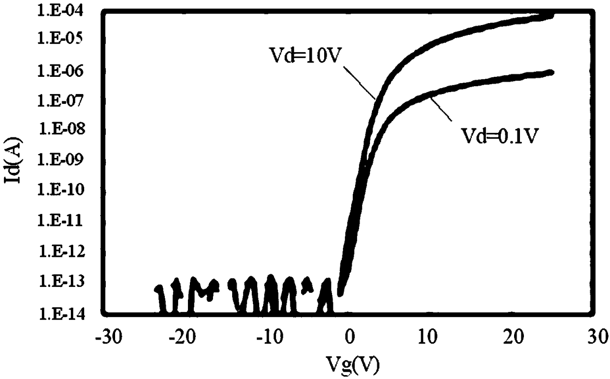
[0042] Specifically, the switching thin film field effect transistor T1 has a first active layer 9 for reducing the subthreshold swing of the transfer characteristic curve of the switching thin film field effect transistor T1. In addition, the driving thin film field effect transistor T2 has a second active layer 10 for increasing the sub-threshold swing of the transfer characteristic curve of the driving thin film field effect transistor T2.
[0043] The first active layer 9 c...
Embodiment 2
[0046] The organic light emitting display device of this embodiment includes a switching thin film field effect transistor T1, a driving thin film field effect transistor T2, and storage capacitors respectively connected to the switching thin film field effect transistor T1 and the driving thin film field effect transistor T2.
[0047] Specifically, the switching thin film field effect transistor T1 has a first active layer 9 for reducing the subthreshold swing of the transfer characteristic curve of the switching thin film field effect transistor T1. In addition, the driving thin film field effect transistor T2 has a second active layer 10 for increasing the sub-threshold swing of the transfer characteristic curve of the driving thin film field effect transistor T2.
[0048] Compared with the first embodiment, the oxygen content of the second active layer 10 of the organic light emitting display device of this embodiment is higher than the oxygen content of the first active layer 9...
Embodiment 3
[0051] The organic light emitting display device of this embodiment includes a switching thin film field effect transistor T1, a driving thin film field effect transistor T2, and storage capacitors respectively connected to the switching thin film field effect transistor T1 and the driving thin film field effect transistor T2.
[0052] Specifically, the switching thin film field effect transistor T1 has a first active layer 9 for reducing the subthreshold swing of the transfer characteristic curve of the switching thin film field effect transistor T1. In addition, the driving thin film field effect transistor T2 has a second active layer 10 for increasing the sub-threshold swing of the transfer characteristic curve of the driving thin film field effect transistor T2. The oxygen content of the second active layer 10 is higher than the oxygen content of the first active layer 9.
[0053] Compared with the second embodiment, the first active layer 9 and the second active layer 10 of t...
PUM
 Abstract
Description
Claims
Application Information
 - R&D Engineer
- R&D Manager
- IP Professional
- Industry Leading Data Capabilities
- Powerful AI technology
- Patent DNA Extraction
Browse by: Latest US Patents, China's latest patents, Technical Efficacy Thesaurus, Application Domain, Technology Topic, Popular Technical Reports.
© 2024 PatSnap. All rights reserved.Legal|Privacy policy|Modern Slavery Act Transparency Statement|Sitemap|About US| Contact US: help@patsnap.com