A kind of thick-film SOI-LIGBT device and its anti-latch-up improving method
A device and thick film technology, applied in the fields of semiconductor devices, semiconductor/solid-state device manufacturing, electrical components, etc., can solve the problem that the device cannot be turned off, improve the latch-up resistance, reduce the voltage drop, and reduce the possibility of latch-up sexual effect
- Summary
- Abstract
- Description
- Claims
- Application Information
AI Technical Summary
Problems solved by technology
Method used
Image
Examples
Embodiment 1
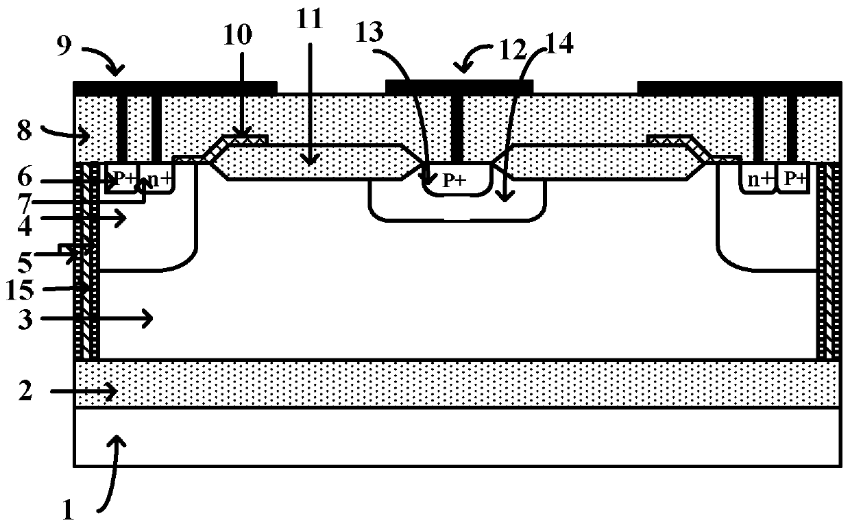
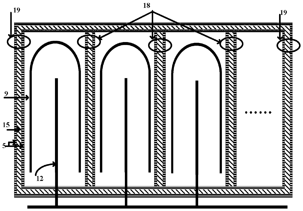
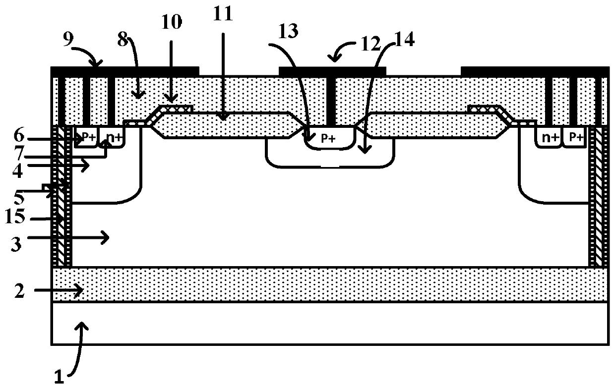
[0021] A thick-film SOI-LIGBT device, comprising a P-type substrate 1, a layer of buried oxide layer 2 is arranged on the P-type substrate 1, an N-type drift region 3 is arranged above the buried oxide layer 2, and the N-type drift region 3 P-type body region 4 and N-type buffer zone 14 are provided inside, and P-type cathode contact region 6 and n-type cathode contact region 7 are arranged on the surface of P-type body region 4, and P-type cathode contact region 6 and n-type cathode contact region 7 is connected to the cathode contact metal layer 9, a P-type anode contact region 13 is provided on the surface of the N-type buffer zone 14, the P-type anode contact region 13 is connected to the anode contact metal layer 12, and the surface of the N-type drift region 3 has field oxidation Layer 11 and conductive polysilicon gate 10, field oxide layer 11 is between n-type cathode contact region 7 and P-type contact region 13, conductive polysilicon gate 10 extends from the boundary...
Embodiment 2
[0023]A method for improving the latch-up resistance of the thick-film SOI-LIGBT device, the SOI-LIGBT device includes a P-type substrate 1, a layer of buried oxide layer 2 is arranged on the P-type substrate 1, and the buried oxide There is an N-type drift region 3 above the layer 2, and a P-type body region 4 and an N-type buffer zone 14 are arranged inside the N-type drift region 3, and a P-type cathode contact region 6 and an n-type cathode are arranged on the surface of the P-type body region 4 The contact area 7, the P-type cathode contact area 6 and the n-type cathode contact area 7 are connected to the cathode contact metal layer 9, and the surface of the N-type buffer zone 14 is provided with a P-type anode contact area 13, and the P-type anode contact area 13 is connected to the anode The contact metal layer 12 is connected, the surface of the N-type drift region 3 has a field oxide layer 11 and a conductive polysilicon gate 10, the field oxide layer 11 is between the...
PUM
 Abstract
Description
Claims
Application Information
 - R&D Engineer
- R&D Manager
- IP Professional
- Industry Leading Data Capabilities
- Powerful AI technology
- Patent DNA Extraction
Browse by: Latest US Patents, China's latest patents, Technical Efficacy Thesaurus, Application Domain, Technology Topic, Popular Technical Reports.
© 2024 PatSnap. All rights reserved.Legal|Privacy policy|Modern Slavery Act Transparency Statement|Sitemap|About US| Contact US: help@patsnap.com


