
Additive for polycrystalline silicon wafer texturization and application method thereof

A polycrystalline silicon wafer and additive technology, applied in the field of solar cells, can solve the problems of difficult removal, decreased conversion efficiency, metal pollution, etc., and achieve the effects of improving the texturing effect and stably increasing the conversion efficiency.

Inactive Publication Date: 2016-12-14
杭州飞鹿新能源科技有限公司
View PDF10 Cites 12 Cited by
  • Summary
  • Abstract
  • Description
  • Claims
  • Application Information

AI Technical Summary

Problems solved by technology

However, due to the strong adsorption of organic components in the additive, there will be organic residues on the surface of the silicon wafer, and it is difficult to remove the subsequent alkaline and pickling, so that it is in a hydrophilic state, making it difficult to dry the silicon wafer and easily introduce metal pollution. This leads to a decrease in the parallel resistance and open circuit voltage of the battery, and ultimately leads to a limited increase in the conversion efficiency of the battery sheet, or even a decrease
At the same time, the addition of additives leads to the formation of porous silicon inside the textured surface, which will also significantly affect the subsequent diffusion and coating processes, resulting in an increase in the failure rate and a decrease in conversion efficiency.

Method used


Image

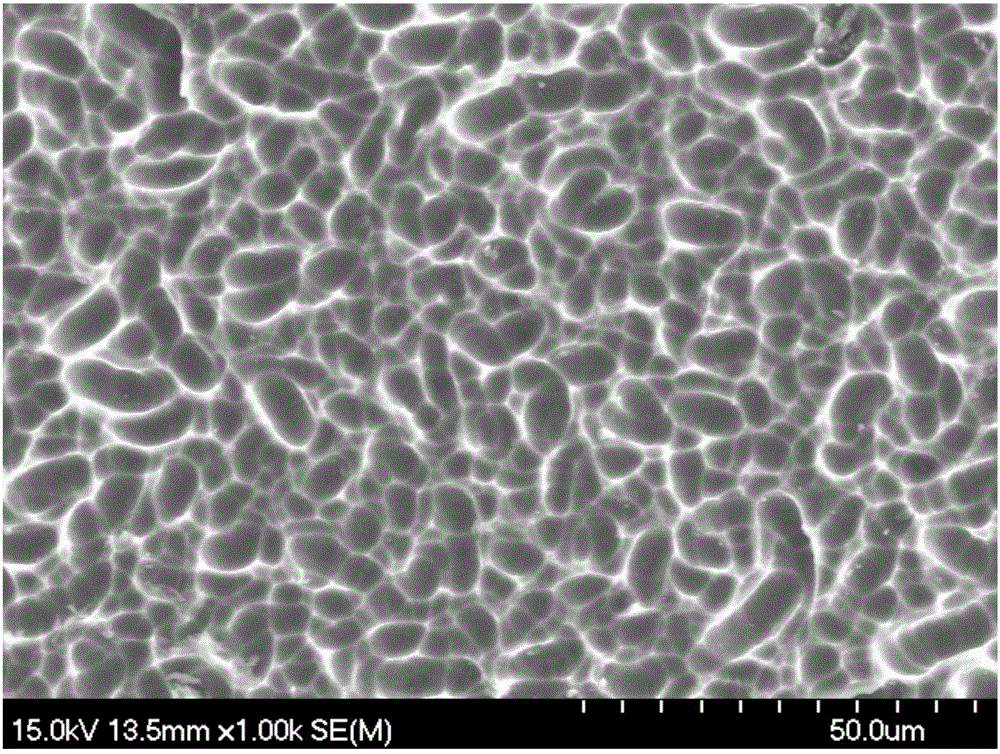
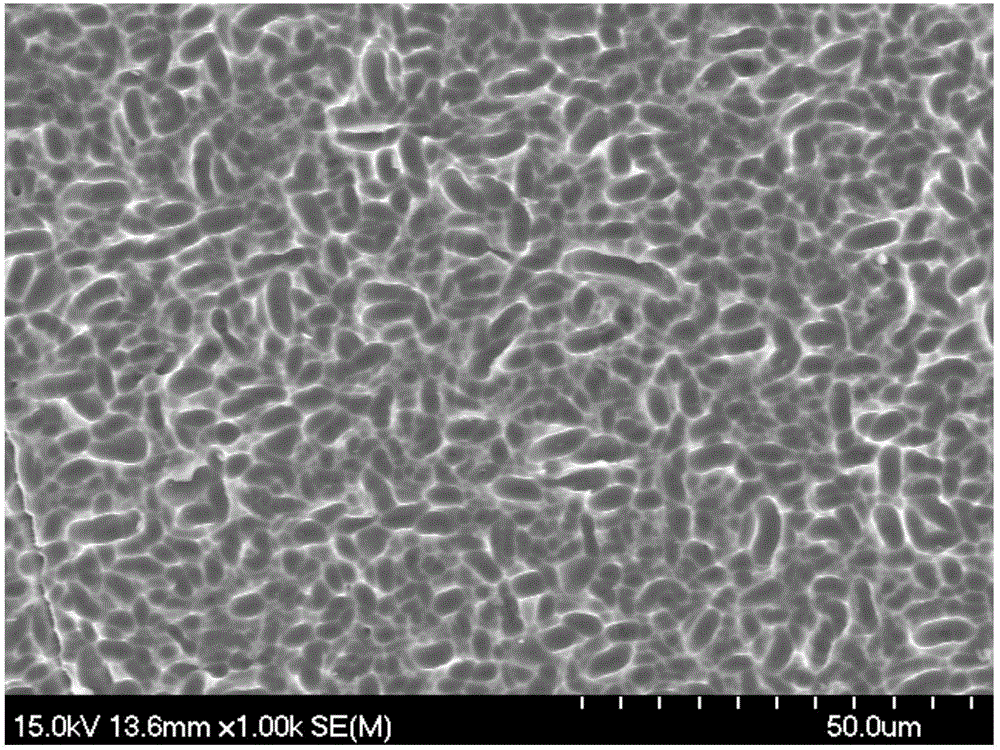
  • Additive for polycrystalline silicon wafer texturization and application method thereof
  • Additive for polycrystalline silicon wafer texturization and application method thereof
  • Additive for polycrystalline silicon wafer texturization and application method thereof

Examples


Embodiment 1

[0027] comparison group

[0028] The current conventional acid cashmere method:

[0029] Prepare acid texturing solution: Add 1.25L of hydrofluoric acid with a concentration of 55%, 5.5L of nitric acid with a concentration of 65-68%, and 3.25L of deionized water into the texturing tank and stir to obtain 10L of acid texturing liquid;

[0030] Acid texturing: put the solar polysilicon wafer into the texturing tank for texturing, the texturing temperature is 7°C, and the texturing time is 90s.

[0031] The reflectance after conventional texturing is 27%.

Embodiment 2

[0033] The additive used in polycrystalline silicon chip texturing and the method for applying the additive to acid texturing adopt the following process steps:

[0034] Configure acid texturing additive: add 10g polyacrylic acid (Mw:3000-5000), 20g succinic acid, 0.5g fatty acid methyl ester ethoxylate (FMEE) into 1000ml deionized water to make polycrystalline texturing additive;

[0035] Prepare acid texturing solution: Add 1.25L of hydrofluoric acid with a concentration of 55%, 5.5L of nitric acid with a concentration of 65-68%, and 3.25L of deionized water into the texturing tank and stir to obtain 10L of acid texturing liquid;

[0036] Add 0.1L of additives to the acid texturing solution prepared in step 2);

[0037] Acid texturing: put the solar polysilicon wafer into the texturing tank for texturing, the texturing temperature is 7°C, and the texturing time is 90s.

[0038] Simultaneously by the method for embodiment 1, make conventional without adding additive of the ...

Embodiment 3

[0045] Applying the additive used for polysilicon chip texturing The method of applying the additive to acid texturing takes the following process steps:

[0046] Configure acid texturing additive: add 10g polyacrylic acid (Mw:3000-5000), 50g oxalic acid, 0.5g fatty acid methyl ester ethoxylate (FMEE) into 1000ml deionized water to make polycrystalline texturing additive;

[0047] Prepare acid texturing solution: Add 1.25L of hydrofluoric acid with a concentration of 55%, 5.5L of nitric acid with a concentration of 65-68%, and 3.25L of deionized water into the texturing tank and stir to obtain 10L of acid texturing liquid;

[0048] Add 0.1L of additives to the acid texturing solution prepared in step 2);

[0049] Acid texturing: put the solar polysilicon wafer into the texturing tank for texturing, the texturing temperature is 7°C, and the texturing time is 90s.

[0050] Simultaneously by the method for embodiment 1, make conventional without adding additive of the present i...


PUM

PropertyMeasurementUnit
degree of polymerizationaaaaaaaaaa
reflectanceaaaaaaaaaa

Abstract

The invention provides an additive for polycrystalline silicon wafer texturization and a method of applying the additive to perform texturization. The additive is prepared from polymer carboxylic acid, micromolecular organic acid, non-ionic surfactant and water, wherein the weight ratio of the polymer carboxylic acid to the water is 0.5-5 to 100, the weight ratio of the micromolecular organic acid to the water ratio is 1-10 to 100, and the weight ratio of the non-ionic surfactant to the water is 0.01-1 to 100. The texturization is performed by using the additive, the uniformity of suede can be improved, further polycrystalline silicon wafer reflectivity is reduced, and the side effects such as silicon wafer surface contamination and suede inside porous silicon are not produced.

Description

technical field [0001] The invention relates to an additive for making texture of a polycrystalline silicon wafer and an application method thereof, belonging to the technical field of solar cells. Background technique [0002] With the development of photovoltaic technology, the efficiency of polycrystalline silicon solar cells has been significantly improved while maintaining low prices. In terms of power stations, its advantages are even more obvious. Therefore, the proportion of polycrystalline batteries on the market has far exceeded that of monocrystalline batteries. [0003] For polycrystalline silicon solar cells, the crystallographic orientation varies across the surface. If the anisotropic alkali etching method used in monocrystalline silicon is used, a surface texture similar to steps will be formed. This kind of surface texture can not get the ideal anti-reflection effect, which is not conducive to the absorption of light. Therefore, HF-HNO is widely used to e...

Claims


Application Information

Patent Timeline
Patent Type & Authority Applications(China)
IPC IPC(8): C30B33/10C30B29/06H01L31/18
CPCC30B29/06C30B33/10H01L31/182Y02P70/50
Inventor 夏庆华斯小阳姚伟明
Owner 杭州飞鹿新能源科技有限公司
Learn More