
Display panel and preparation method

A technology of display panel and phase separation method, which is applied in the fields of final product manufacturing, sustainable manufacturing/processing, semiconductor/solid-state device manufacturing, etc. It can solve the problems of water-blocking layer fracture and poor flexibility, so as to improve water-blocking performance and possibility The effect of reducing and changing the process steps less

Active Publication Date: 2016-12-07
BOE TECH GRP CO LTD
View PDF13 Cites 18 Cited by
  • Summary
  • Abstract
  • Description
  • Claims
  • Application Information

AI Technical Summary

Problems solved by technology

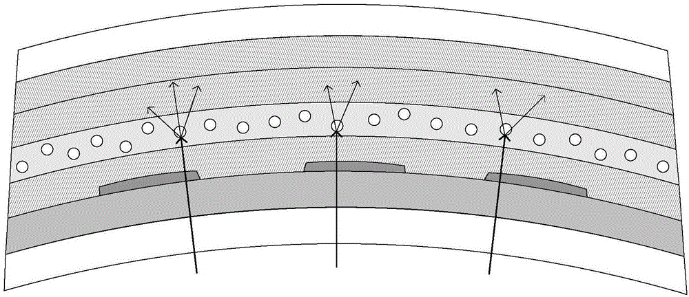
[0005] Embodiments of the present invention provide a display panel and a preparation method thereof, which are used to disperse the force on the stress-bearing surface of the water-blocking layer during the bending process through the droplet microstructure in the organic buffer layer, thereby improving the stress-bearing surface of the water-blocking layer. The stress on the force surface is relatively concentrated, and the water-blocking layer is broken due to the poor flexibility of the water-blocking layer, and a new water molecule erosion channel is formed at the fracture; and the water molecule penetration is prolonged through the micro-droplet microstructure in the organic buffer layer The path prolongs the time for water molecules to reach the light-emitting layer in the display panel, improving the device life of the light-emitting layer

Method used


Image

  • Display panel and preparation method
  • Display panel and preparation method
  • Display panel and preparation method

Examples


Embodiment Construction

[0039] The embodiment of the present invention provides a display panel and a preparation method, which are used to disperse the stress on the stressed surface of the inorganic water-blocking layer during the bending process through the droplet microstructure in the organic buffer layer, and improve the performance of the inorganic water-blocking layer. The stress on the stress-bearing surface is relatively concentrated, and the inorganic water-blocking layer is broken due to the poor flexibility of the inorganic water-blocking layer, and a new water molecule erosion channel is formed at the fracture; and the droplet microstructure in the organic buffer layer Prolonging the penetration path of water molecules prolongs the time for water molecules to reach the light-emitting layer in the display panel, which improves the device life of the light-emitting layer; the display panel provided by the embodiment of the present invention has better water resistance than the display panel...


PUM


Abstract

The invention provides a display panel and a preparation method. The stress of stress faces of water resisting layers in the buckling process is dispersed through a microdroplet microstructure in an organic buffer layer, and the problems that the stress of the stress faces of the water resisting layers is centralized and the problem that due to water resisting layer fracture caused by the toughness difference of the water resisting layers, new water molecule corrosion channels are formed at fracture positions are changed. The microdroplet microstructure in the organic buffer layer lengthen the path of water molecule permeation, the time for water molecules to reach a light emitting layer in the display panel is prolonged, and the service life of devices of the light emitting layer is prolonged. The display panel comprises the first inorganic water resisting layer, the second inorganic water resisting layer and the organic buffer layer located between the first inorganic water resisting layer and the second water resisting layer. The organic buffer layer comprises the microdroplet microstructure used for dispersing stress of the organic buffer layers.

Description

technical field [0001] The invention relates to the field of display technology, in particular to a display panel and a preparation method. Background technique [0002] Organic Light-Emitting Diode (OLED) has the characteristics of self-luminescence, high brightness, high contrast, low operating voltage, and flexible display, and is known as the most promising display device. [0003] see figure 1 , the existing display panel includes: a flexible substrate 101, a thin film transistor 102, a light emitting layer 103, a first inorganic water blocking layer 104, an organic buffer layer 105, a second inorganic water blocking layer 106, a barrier layer 107, and a glass cover 108. In order to prevent the light-emitting layer 103 from being corroded by water and oxygen in the OLED device, a common method is to use a hard substrate with high water resistance (such as glass) for encapsulation. But this scheme is not suitable for flexible OLED devices. For flexible OLED devices, t...

Claims


Application Information

Patent Timeline
IPC IPC(8): H01L51/52H01L51/56
CPCH10K50/841H10K50/844H10K2102/311H10K71/00Y02E10/549Y02P70/50H10K71/12H10K59/12H10K77/111H10K59/1201
Inventor 宋平王菲菲王有为蔡鹏敏健
Owner BOE TECH GRP CO LTD
Learn More