


Quick Research
Generate reliable direction feasibility study reports for your R&D in just a few steps.

Technical Q&A
Discover and master advanced knowledge NOW. Basics, ideas, possibilities, all at once.

Find Solutions
As an expert in R&D theories, this can generate solutions to your technical problems instantly.

Evaluate Feasibility
Analyze your overall solution with one click, know your potential R&D risks in advance.

Monitor Landscape
Get weekly tech updates, stay abreast of the latest tech innovations and key insights.
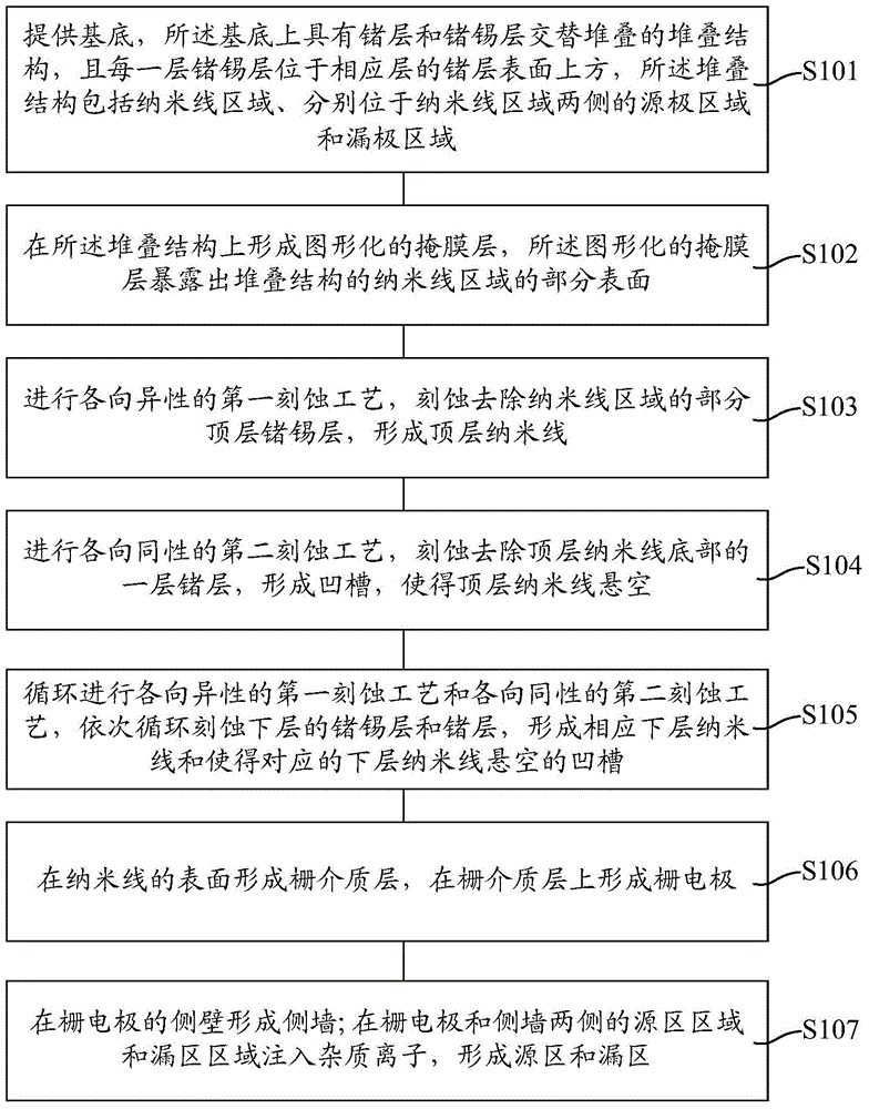
Formation method of nanowire field effect transistor
A field effect transistor and nanowire technology, which is applied in the field of semiconductor manufacturing, can solve the problem that the performance of the nanowire field effect transistor needs to be improved, and achieves the effect of maintaining stable etching process parameters and improving performance.
- Summary
- Abstract
- Description
- Claims
- Application Information
AI Technical Summary
Problems solved by technology
Method used
Image


Examples
Embodiment Construction
[0033] The performance of the nanowire field effect transistor formed by the prior art still needs to be improved. For example, the prior art is prone to etching damage during the process of forming the nanowire, and the shape of the nanowire is not easy to control.
[0034] Research has found that the single-crystal silicon germanium layer and the single-crystal silicon layer in the stacked structure, as well as the single-crystal silicon layer and the buried layer in the SOI substrate are patterned using a plasma etching process, and the etching gas used in the plasma etching process is for Cl 2 , the plasma damages the nanowires under the acceleration of the electric field; in addition, the patterning of the stacking result is a one-step etching. Since the materials of each layer in the stacking structure are different, the etching process is more complicated. The etching process The parameters are difficult to keep stable, so it is difficult to maintain the same size of th...
PUM
| Property | Measurement | Unit |
|---|---|---|
| thickness | aaaaa | aaaaa |
| thickness | aaaaa | aaaaa |
Abstract
Description
Claims
Application Information
 - R&D Engineer
- R&D Manager
- IP Professional
- Industry Leading Data Capabilities
- Powerful AI technology
- Patent DNA Extraction
Browse by: Latest US Patents, China's latest patents, Technical Efficacy Thesaurus, Application Domain, Technology Topic, Popular Technical Reports.
© 2024 PatSnap. All rights reserved.Legal|Privacy policy|Modern Slavery Act Transparency Statement|Sitemap|About US| Contact US: help@patsnap.com