A carrier assembly for ceramic packaging power devices and its manufacturing method

A power device and ceramic packaging technology, which is applied in the manufacture of printed circuits, assembly of printed circuits with electrical components, electrical components, etc., can solve the problem of relatively high processing precision of heat conduction blocks, large influence of heat conduction of power devices, and variable heat dissipation capacity of power devices. To achieve the effect of solving heat conduction and stress matching problems, lowering temperature, and reducing stress

Active Publication Date: 2011-05-25
BEIJING SATELLITE MFG FACTORY
View PDF0 Cites 0 Cited by
  • Summary
  • Abstract
  • Description
  • Claims
  • Application Information

AI Technical Summary

Problems solved by technology

The method of directly installing power devices on the chassis structural board is only suitable for metal packaged power devices with mounting holes; the aluminum substrate installation method has poor reliability due to the large difference in thermal expansion coefficient between the ceramic packaged power device and the aluminum substrate; structural parts The boss installation method directly installs the power device on the printed board, and then installs the printed board on the boss. Since the distance between the printed board and the boss is difficult to control, the heat conduction of the power device is affected by the process. Larger, and with the increase of the working time of electronic equipment, the deformation of the printed board will lead to the deterioration of the heat dissipation capacity of the power device, affecting the design life; the installation method of processing a specific heat conduction block requires a specific installation method for specific power devices , requires a large installation space, it is easy to generate installation stress during installation, and the processing accuracy of the heat conduction block is relatively high

Method used


Image

  • A carrier assembly for ceramic packaging power devices and its manufacturing method
  • A carrier assembly for ceramic packaging power devices and its manufacturing method
  • A carrier assembly for ceramic packaging power devices and its manufacturing method

Examples


Embodiment Construction

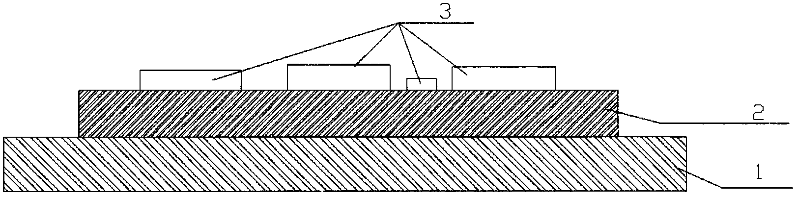
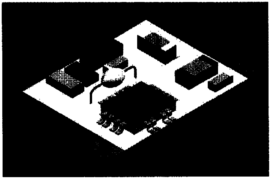
[0026] Such as figure 1 As shown, the carrier assembly of the present invention includes a ceramic circuit board and a carrier assembly substrate; the ceramic circuit board is coated with copper on both sides, and the back of the circuit board is spaced with a ventilation groove; the carrier assembly substrate is made of molybdenum copper material, and the upper surface of the substrate The surface is electroplated with lead-tin alloy; the ceramic circuit board and the substrate of the carrier component are welded together with lead-tin alloy.

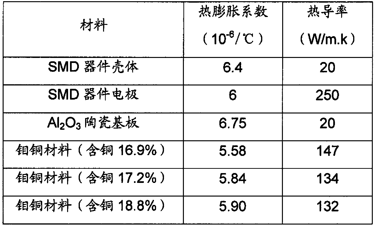
[0027] In order to ensure that the material of the substrate of the carrier assembly has a similar thermal expansion coefficient and conductivity to ceramics and SMD power devices packaged in ceramics, the thermal expansion coefficients and thermal conductivity of several materials shown in the table below are obtained according to experiments. By comparison, molybdenum-copper alloy is selected as the raw material of the substrate of t...


PUM

PropertyMeasurementUnit
thicknessaaaaaaaaaa
thicknessaaaaaaaaaa
thicknessaaaaaaaaaa

Abstract

A carrier assembly for ceramic packaged power devices and a manufacturing method thereof. Molybdenum copper alloy is selected as the mounting carrier material, and the linear expansion coefficient matching relationship between the ceramic packaged power device shell material, the ceramic substrate material and the mounting carrier material is utilized. The carrier component is formed by vacuum brazing and ceramic circuit board manufacturing process. In addition to meeting stress matching, various materials also have high thermal conductivity. The formed carrier component has good heat conduction effect, ensuring low thermal resistance and low stress installation. Require. This kind of carrier component can be designed according to the specific requirements of power devices, and combined with electronic equipment circuits to form high-reliability power electronic products.

Description

technical field [0001] The invention relates to a carrier component and a manufacturing method thereof, in particular to a carrier component for ceramic packaged power devices and a manufacturing method thereof. Background technique [0002] With the rapid development of aerospace technology, the power of the spacecraft power supply system continues to increase, the power of communication satellites has increased from 2 to 3kW to 8 to 10kW, and the power of the latest generation of large-capacity communication satellites will reach 20 to 30kW, and the design life is also It will be increased from 8 years to 15 years; moreover, in order to reduce the launch cost of the satellite and increase the capacity of the payload, it is required to continuously reduce the size and weight of the electronic equipment on the satellite, which leads to the shortage of high-power devices for power supply stand-alone products. Thermal design issues are very prominent. [0003] In order to sol...

Claims


Application Information

Patent Timeline
Patent Type & Authority Patents(China)
IPC IPC(8): H05K1/00H05K3/00H05K3/34
Inventor 万成安时娇健徐珩衍李廷中徐京新陈尚达
Owner BEIJING SATELLITE MFG FACTORY
Why Eureka
Try Eureka