Optical thin film with random pyramid morphology texture and its preparation method
A technology of optical thin film and pyramid, applied in semiconductor/solid-state device manufacturing, electrical components, electric solid-state devices, etc., can solve problems such as high cost, complex process, and distortion of emission spectrum, and achieve low manufacturing cost, simple operation, and low cost Effect
- Summary
- Abstract
- Description
- Claims
- Application Information
AI Technical Summary
Problems solved by technology
Method used
Image
Examples
Embodiment 1
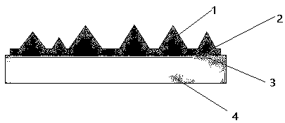
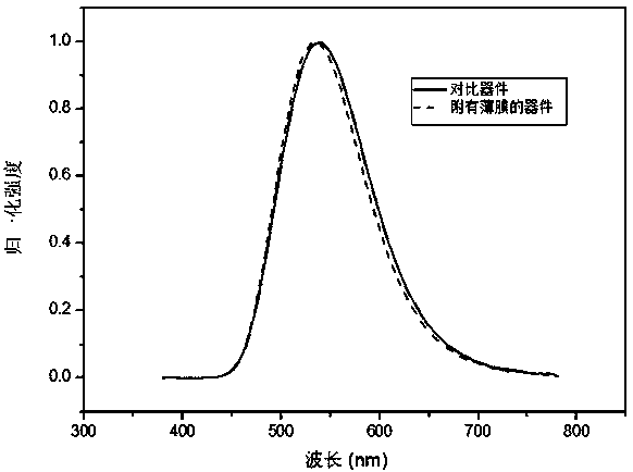
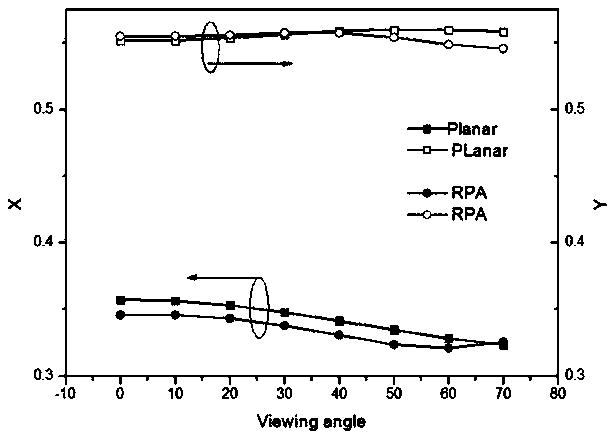
[0026] In this example, see Figure 1~3 , a kind of optical thin film with random pyramid appearance suede, comprising a transparent substrate 2 of the optical film, one side surface of the transparent base 2 has a random pyramid appearance suede 1, the random pyramid appearance suede 1 is composed of a series of The pyramid-shaped structure with uneven size and position forms a pyramid array arranged randomly, forming a non-planar light-scattering functional structural layer, and the other side surface of the transparent substrate 2 forms a bottom connecting layer 3 that can be closely connected with the OLED substrate 4. Each pyramid of the random pyramid shaped suede 1 is a cone with four upper surfaces. The size and height of the pyramids of the suede surface 1 with the random pyramid shape are 2-10 microns. The apex angle of each pyramid of the suede surface 1 of the random pyramid shape is 80°-100°. The transparent substrate 2 is made of NOA63 optical glue. The connec...
Embodiment 2
[0033] This embodiment is basically the same as Embodiment 1, especially in that:
[0034] In this embodiment, Ausbond3301 optical glue is used as the main material of the optical film.
[0035] In this embodiment, the preparation method of the optical film with a random pyramid shape suede in this embodiment is prepared by a two-step transfer printing method, and the specific steps are as follows:
[0036] a. This step is identical with embodiment one;
[0037] b. This step is identical with embodiment one;
[0038] c. Transfer process of random pyramid texture: the structure of OLED device is ITO(100nm) / MoO 3 (5nm) / NPB(60nm) / Alq3(60nm) / LiF(0.5nm) / Al(100nm) OLED device, when the pixel size of the device is 5mm*5mm, Ausbond3301 optical glue is used as the body material of the optical film, Apply Ausbond3301 optical glue on the PDMS film prepared in step b and stick it on the surface of the OLED glass substrate. Using the PDMS soft template with inverted pyramid structure pr...
Embodiment 3
[0042] This embodiment is basically the same as the previous embodiment, and the special features are:
[0043] In this embodiment, NOA63 optical glue is used as the bulk material of the optical film.
[0044] In this embodiment, the preparation method of the optical film with a random pyramid shape suede in this embodiment is prepared by a two-step transfer printing method, and the specific steps are as follows:
[0045] a. The manufacturing process of the template with random pyramid suede: a single crystal silicon wafer with a P-type resistance of 1-5Ω (100) crystal orientation is used as the template substrate, and the single crystal silicon wafer (100) is washed with acetone, alcohol, Ultrasonic cleaning with deionized water. After cleaning, use 5% HF to remove the natural oxide layer on the surface, and then clean it with a large amount of deionized water. Using alkaline solution as an etchant, place the cleaned silicon wafer at a mass concentration of In a mixed soluti...
PUM
 Abstract
Description
Claims
Application Information
 - Generate Ideas
- Intellectual Property
- Life Sciences
- Materials
- Tech Scout
- Unparalleled Data Quality
- Higher Quality Content
- 60% Fewer Hallucinations
Browse by: Latest US Patents, China's latest patents, Technical Efficacy Thesaurus, Application Domain, Technology Topic, Popular Technical Reports.
© 2025 PatSnap. All rights reserved.Legal|Privacy policy|Modern Slavery Act Transparency Statement|Sitemap|About US| Contact US: help@patsnap.com


