Method for improving selected area epitaxial growth interface

A technology of selective area epitaxy and interface, which is applied in the direction of electrical components, semiconductor/solid-state device manufacturing, circuits, etc., to achieve the effect of improving crystal quality and low dislocation density

Inactive Publication Date: 2016-10-12
SUN YAT SEN UNIV
View PDF7 Cites 5 Cited by
  • Summary
  • Abstract
  • Description
  • Claims
  • Application Information

AI Technical Summary

Problems solved by technology

Because: (1) The thickness of the epitaxial layer in the selected area is about tens of nanometers, and the conductive channel is near the growth interface, which is easily affected by non-ideal factors at the interface

Method used


Image

  • Method for improving selected area epitaxial growth interface
  • Method for improving selected area epitaxial growth interface
  • Method for improving selected area epitaxial growth interface

Examples


Embodiment 1

[0036] Such as Picture 8 Shown here is a schematic diagram of the selected region epitaxial structure of this embodiment. The structure includes a substrate (1), a stress buffer layer (2), a GaN buffer layer (3), a GaN insertion layer (4), and a GaN trench from bottom to top. Road layer (5), AlGaN barrier layer (6). The manufacturing method of the above-mentioned selective area epitaxial structure is as Figure 1-Figure 8 As shown, including the following steps:

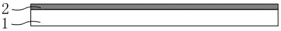
[0037] 1) Provide a substrate (1); such as figure 1 Shown.

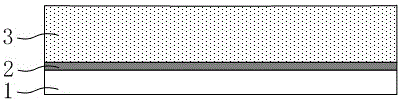
[0038] 2) Growing a stress buffer layer (2) on the substrate (1); such as figure 2 Shown.

[0039] 3) Grow a GaN buffer layer (3) on the stress buffer layer; image 3 Shown.

[0040] 4) Deposit a layer of SiO2 on the GaN buffer layer (3) as a mask layer (7);. Such as Figure 4 Shown.

[0041] 5) Use photolithography and development technology and wet etching to remove the dielectric layer in the area where the epitaxial AlGaN is needed to realize the patterning...


PUM


Abstract

The invention relates to the technical field of semiconductor epitaxial technology, specifically to a method for improving a selected area epitaxial growth interface. The method includes the steps of providing a substrate for epitaxial growth, depositing a stress buffer layer and a GaN buffer layer sequentially on the substrate, obtaining a selected area epitaxial template, depositing a dielectric layer on the template as a mask layer, eroding and removing the dielectric layer on the area where epitaxial AlGaN is needed through lithography development technology and a wet method to realize patterns on the mask layer, depositing low pressure grown GaN interposed layer on the areas which do not masked, and normally growing a GaN channel layer and an AlGaN barrier layer. The method is simple in process, the performance of a selected area epitaxial interface can be effectively improved, and the quality selected area epitaxial layer is also improved. Body leakage current in the epitaxial layer and reverse leakage current of a schottky diode can be reduced.

Description

Technical field [0001] The present invention relates to the technical field of semiconductor epitaxial processes, and more specifically, to a method for improving the interface of selected area epitaxial growth. Background technique [0002] Selective area growth (SAG) technology has a wide range of applications in semiconductor epitaxial growth and device manufacturing. In terms of semiconductor epitaxial growth, SAG technology can be used to achieve lateral epitaxial growth, reducing the density of dislocations penetrating the surface of the material and controlling the crystal quality. In terms of semiconductor device manufacturing, SAG technology can be used for the preparation of special structures in planar processes, such as the base or emitter of HBT, n-type highly doped ohmic contact regions in AlGaN / GaN HFETs, and p-GaN in pn junction HFETs Layers and so on. In 2011, Yuhua Wen et al. also proposed a method for implementing trench gate enhanced devices based on the sel...

Claims


Application Information

Patent Timeline
Patent Type & Authority Applications(China)
IPC IPC(8): H01L21/02
CPCH01L21/02538
Inventor 刘扬李柳暗杨帆
Owner SUN YAT SEN UNIV
Why Eureka
Try Eureka