Novel three-dimensional microwave multi-chip module structure

A microwave multi-chip and component structure technology, applied in electrical components, electric solid-state devices, semiconductor devices, etc., can solve the problems of unsuitable mass production, increased component volume, low production efficiency, etc., to improve system integration, reduce Component volume, the effect of improving production efficiency

Active Publication Date: 2016-09-28
THE 13TH RES INST OF CHINA ELECTRONICS TECH GRP CORP
View PDF10 Cites 5 Cited by
  • Summary
  • Abstract
  • Description
  • Claims
  • Application Information

AI Technical Summary

Problems solved by technology

[0006] (3) The current three-dimensional microwave multi-chip components need to be individually assembled for each component, which has low production efficiency and is not suitable for mass production
[0007] (4) The current three-dimensional microwave multi-chip components use metal partitions to solve the electromagnetic compatibility problems of high-gain amplification links and multi-channel components, which is technically difficult and increases the size of components

Method used


Image

  • Novel three-dimensional microwave multi-chip module structure
  • Novel three-dimensional microwave multi-chip module structure
  • Novel three-dimensional microwave multi-chip module structure

Examples


Embodiment Construction

[0018] The following will clearly and completely describe the technical solutions in the embodiments of the present invention with reference to the accompanying drawings in the embodiments of the present invention. Obviously, the described embodiments are only some, not all, embodiments of the present invention. Based on the embodiments of the present invention, all other embodiments obtained by persons of ordinary skill in the art without creative efforts fall within the protection scope of the present invention.

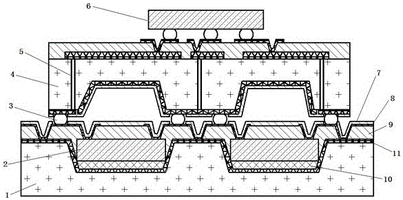
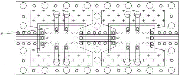
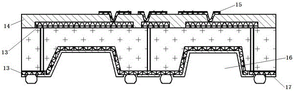
[0019] Such as figure 1 As shown, the present invention discloses a novel three-dimensional microwave multi-chip assembly structure, which includes a bottom silicon chip 1, an MMIC chip 2, a top layer silicon chip 4, and an ASIC chip 6 from bottom to top; the bottom silicon chip 1 is etched with a chip Install groove, and electroplate the first metal layer 11 on the surface, MMIC chip 2 is bonded on the bottom of the chip installation groove by conductive adhesive ...


PUM


Abstract

The invention discloses a novel three-dimensional microwave multi-chip module structure, and relates to the field of microwave microelectronic packaging. The structure comprises a bottom silicon chip, an MMIC chip, a top silicon chip and an ASIC chip from the bottom to the top. The bottom silicon chip is provided with a chip installation groove through etching, and the surface of the bottom silicon chip is plated with a first metal layer. The MMIC chip is bound at the bottom of the chip installation groove through a conductive glue layer, and the upper surface of the MMIC chip and the upper surface of the bottom silicon chip are sequentially provided with a sealed protection layer, a second metal layer and a first solder mask layer. A part, corresponding to the chip installation groove of the bottom silicon chip, of the bottom of the top silicon chip is provided with a bottom groove in an etching manner. The corresponding parts of the bottom and top silicon chips are respectively provided with a welding ball convex point pole in an etching manner. A third solder mask layer of the top silicon chip is provided with a metal electrode in an etching manner, and the ASIC chip is welded on the metal electrode of the top silicon chip. The technological production of a three-dimensional microwave multi-chip module is completed in a mode of wafer level through employing a silicon cavity structure and benzocyclobutene secondary wiring, and the production efficiency is improved.

Description

technical field [0001] The invention relates to the field of microwave microelectronic packaging. Background technique [0002] With the development of microwave and millimeter wave technology, miniaturization, integration and multi-function have become the development direction of RF microwave components. The development of miniaturization and integration is mainly reflected in the following two aspects: (1) the development of multifunctional chips, which can include low-noise amplifiers, drive amplifiers, mixers, filters, switches, digitally controlled attenuators, digitally controlled phase shifters Microwave functional units are integrated on a microwave monolithic integrated circuit (MMIC) to realize the miniaturization of the system, but this method cannot realize the functional integration of chips made of different materials. (2) Using a three-dimensional system integration scheme, the large-scale integrated circuit (ASIC) and MMIC of different materials in the comp...

Claims


Application Information

Patent Timeline
Patent Type & Authority Applications(China)
IPC IPC(8): H01L23/498H01L23/552H01L25/16
CPCH01L24/20H01L2224/04105H01L2224/12105H01L2224/16225H01L2224/16227H01L2224/24137H01L2224/32225H01L2224/73267H01L2924/15153H01L25/162H01L23/49894H01L23/552H01L25/165
Inventor 赵永志王绍东王志强
Owner THE 13TH RES INST OF CHINA ELECTRONICS TECH GRP CORP
Why Eureka
Try Eureka