Method of light-cured resin packaging liquid-state metal printed circuit
A light-curing resin and printed circuit technology, applied in printed circuits, printed circuit manufacturing, printed circuit secondary processing, etc., can solve the problems of packaging thickness and uniformity that are difficult to guarantee, and achieve package specifications that are easy to control and have a wide range of applications. , the effect of improving packaging accuracy and speed
- Summary
- Abstract
- Description
- Claims
- Application Information
AI Technical Summary
Problems solved by technology
Method used
Image
Examples
Embodiment 1
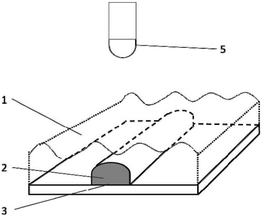
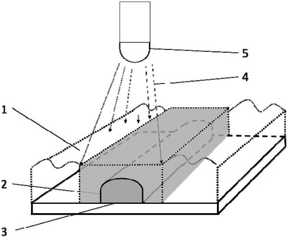
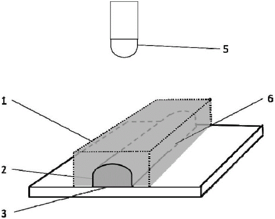
[0036] Figure 1 to Figure 3 It shows the process of encapsulating liquid metal printed circuit with photocuring resin, and the steps include:
[0037] 1) The printed circuit to be packaged is a printed circuit with liquid metal as a wire. Use a dispenser to coat or adhere the photocurable resin in a liquid state to the surface of the liquid metal printed circuit. In this embodiment, the coating thickness is 0.5mm. Liquid metal wires can be connected with electronic components such as semiconductor chips, capacitors, resistors, diodes, and triodes to form functional circuits;
[0038] The liquid metal 2 is a Wood's alloy containing indium, which is an alloy of 50% bismuth, 25% lead, 12.5% tin, and 12.5% cadmium. A printed circuit 3 made of liquid metal is attached to a substrate, which is a rigid substrate 7 ( Figure 4 ), made of rigid plastic.
[0039] 2) The irradiation machine 5 irradiates the light 4 of a specific wavelength onto the photocurable resin 1 on the su...
Embodiment 2
[0042] 1) The printed circuit to be packaged is a printed circuit with liquid metal as a wire. Use a dispenser to coat or adhere the photocurable resin in a liquid state to the surface of the liquid metal printed circuit. The specific coating process and coating thickness are the same as Example 1 is the same.
[0043] Liquid metal 2 is a low melting point gallium indium alloy Ga 80 In 20 . The printed circuit 3 made of liquid metal is attached to the substrate, which is a flexible substrate 8 ( Figure 5 ), made of silicone.
[0044] 2) The irradiation machine 5 irradiates the light 4 of a specific wavelength onto the photocurable resin on the surface of the liquid metal printed circuit ( Figure 6 ), the irradiated photocurable resin is transformed from a liquid state into a solid state by a chemical reaction, and is closely combined with the liquid metal printed circuit, covering the liquid metal wire, forming a protection for the wire, and realizing the packaging of th...
Embodiment 3
[0048] see Figure 7 , step 2) is: the irradiation machine 5 is located under the substrate, and during the packaging process, the irradiation machine 5 irradiates the light 4 of a specific wavelength through the transparent flexible substrate (the substrate material is a PVC film) onto the liquid photocurable resin 1 on the surface of the printed circuit 3 , the final packaging structure is obtained after the irradiated resin is cured and the excess resin material is removed
[0049] Other operations are the same as in Example 1.
PUM
| Property | Measurement | Unit |
|---|---|---|
| wavelength | aaaaa | aaaaa |
Abstract
Description
Claims
Application Information
 - R&D
- Intellectual Property
- Life Sciences
- Materials
- Tech Scout
- Unparalleled Data Quality
- Higher Quality Content
- 60% Fewer Hallucinations
Browse by: Latest US Patents, China's latest patents, Technical Efficacy Thesaurus, Application Domain, Technology Topic, Popular Technical Reports.
© 2025 PatSnap. All rights reserved.Legal|Privacy policy|Modern Slavery Act Transparency Statement|Sitemap|About US| Contact US: help@patsnap.com


