Method of preparing warp-free group-III nitride composite substrate and substrate placing device
A composite substrate and nitride technology, which is applied in semiconductor devices, electrical components, circuits, etc., can solve the problems that affect the material growth device preparation process, warping, etc., to ensure uniformity, improve crystal quality, and reduce production costs. Effect
- Summary
- Abstract
- Description
- Claims
- Application Information
AI Technical Summary
Problems solved by technology
Method used
Image
Examples
Embodiment 1
[0032] Embodiment 1. Preparation of c-plane GaN thick film substrate by HVPE method:
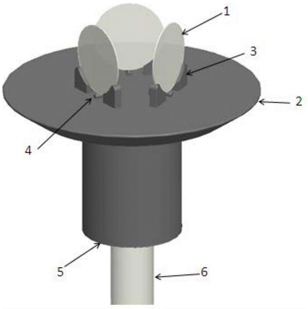
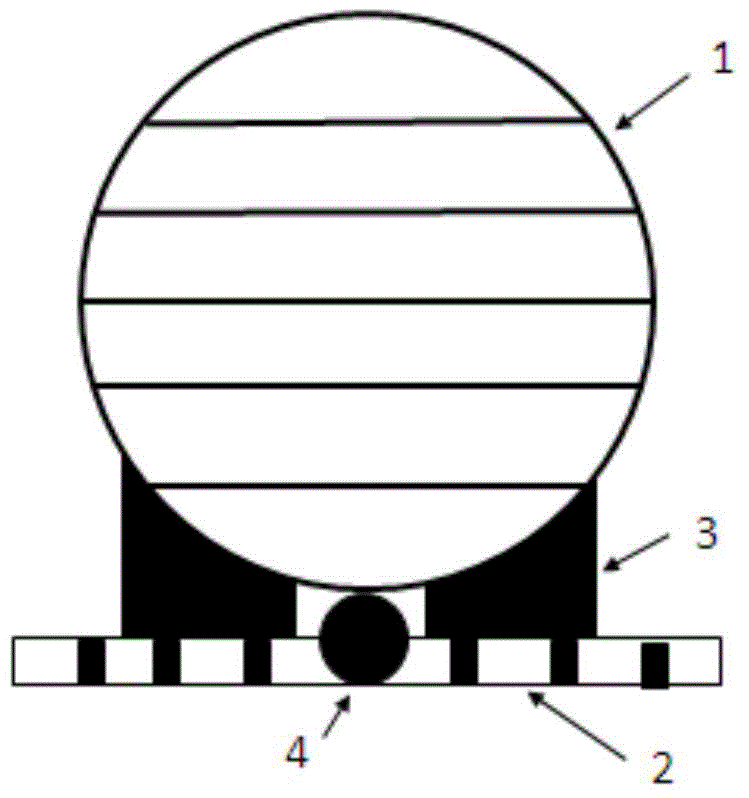
[0033] 1) The graphite frame is designed to stand the double-sided substrate upright in the HVPE reaction chamber for simultaneous epitaxial growth on both sides. When placing the sapphire substrate, make the Al side face the edge of the disk;
[0034] In addition to the sapphire substrate, the double-sided substrate can also be other materials that can realize GaN growth, such as silicon carbide substrate, GaN substrate, Si substrate, LiAlO 2 Substrate etc.
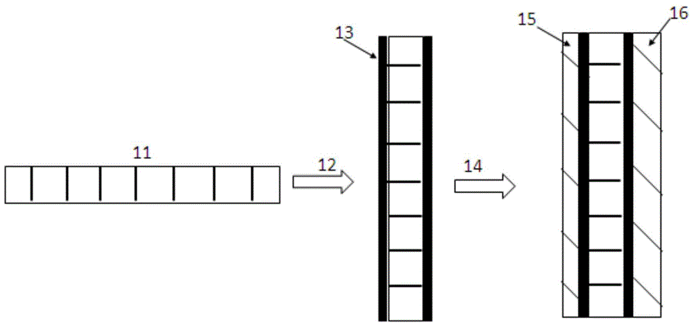
[0035] 2) Epitaxial thin films or microstructures with a certain thickness on both sides of the substrate;
[0036] On the above substrate, epitaxial growth equipment (HVPE, MOCVD, MBE, magnetron sputtering, etc.) is used to form a certain thickness of GaN, InGaN, AlGaN, AlN, InN thin film or microstructure on both sides of the substrate. In this embodiment, HVPE equipment is used to epitaxially GaN thin film structures on both sides...
Embodiment 2
[0042] Embodiment 2, MOCVD growth non-polar a-plane thick-film GaN composite substrate:
[0043] 1) The graphite rack is designed to stand the double-sided substrate upright in the MOCVD reaction chamber for simultaneous epitaxial growth on both sides, and place the substrate so that the Al side faces the edge of the disk;
[0044] The double-sided substrate: can be r-plane sapphire, silicon carbide, Si and other substrates. In this embodiment, the r-plane sapphire substrate is selected, and the a-plane GaN is obtained from the r-plane sapphire epitaxy by the method of the present invention.
[0045] 2) Epitaxial thin films or microstructures with a certain thickness on both sides of the substrate;
[0046] On the above substrate, use the MBE growth technology to grow InN nano-column structures on both sides of the substrate successively to form a transition layer. The growth temperature range of InN nanopillars is 350-500°C, 400°C is used in this embodiment; the height is 10...
Embodiment 3
[0052] Embodiment 3. Preparation of non-polar m-plane GaN thick film substrate by magnetron sputtering method:
[0053] 1) The graphite frame is designed to stand the double-sided substrate upright in the magnetron sputtering reaction chamber for simultaneous epitaxial growth on both sides. When placing the substrate, the Al side faces the edge of the disk;
[0054] The substrate is polished on both sides, which can be Y-LiAlO 2 , silicon carbide, Si and other substrates;
[0055] 2) Epitaxial thin films or microstructures with a certain thickness on both sides of the substrate;
[0056] The above substrate was grown on both sides of the substrate by MOCVD growth technology. 0.05 Ga 0.95 The transition layer of the N nanopillar structure. al 0.05 Ga 0.95 The height of N nanopillars is 200nm-500nm, 300nm is used in this embodiment, and the growth temperature is 1050-1200°C, 1100°C is used in this embodiment.
[0057] 3) An m-plane GaN material is grown on the transition ...
PUM
| Property | Measurement | Unit |
|---|---|---|
| Thickness | aaaaa | aaaaa |
| Thickness | aaaaa | aaaaa |
| Thickness | aaaaa | aaaaa |
Abstract
Description
Claims
Application Information
 - R&D Engineer
- R&D Manager
- IP Professional
- Industry Leading Data Capabilities
- Powerful AI technology
- Patent DNA Extraction
Browse by: Latest US Patents, China's latest patents, Technical Efficacy Thesaurus, Application Domain, Technology Topic, Popular Technical Reports.
© 2024 PatSnap. All rights reserved.Legal|Privacy policy|Modern Slavery Act Transparency Statement|Sitemap|About US| Contact US: help@patsnap.com


