A method for manufacturing an inner layer copper plate exposed copper of a power battery circuit board
What is Al technical title?
Al technical title is built by PatSnap Al team. It summarizes the technical point description of the patent document.
A technology of power battery and manufacturing method, which is applied in the directions of secondary treatment of printed circuit, application of non-metallic protective layer, and formation of electrical connection of printed components, etc. Glue and other problems, to achieve the effect of improving production efficiency, high cutting efficiency, and reducing production costs
Active Publication Date: 2019-01-15
VICTORY GIANT TECH HUIZHOU CO LTD
View PDF4 Cites 0 Cited by
Summary
Abstract
Description
Claims
Application Information
AI Technical Summary
This helps you quickly interpret patents by identifying the three key elements:
Problems solved by technology
Method used
Benefits of technology
Problems solved by technology
[0003] Since the power battery circuit board needs to carry large current and high voltage, ordinary circuit boards can no longer meet this requirement. It is necessary to embed a certain thickness of copper plate in the circuit board, and a small part of the inner copper plate of the finished circuit board needs to be exposed for current output. , thus greatly increasing the difficulty of making circuit boards
In addition, in traditional processing, since the inner layer copper plate will be covered by the prepreg when it is pressed, the position where the inner layer copper plate is exposed needs to be made by controlled depth milling. Because the depth of controlled deep milling is not easy to control, it is easy to damage the copper, and the efficiency Low and there will be residual glue in the prepreg
Method used
Image
Click on the blue label to locate the original text in one second.
Reading with bidirectional positioning of images and text.
Examples
Embodiment Construction
[0022] In order to allow those skilled in the art to better understand the technical solutions of the present invention, the present invention will be further described below in conjunction with the accompanying drawings.
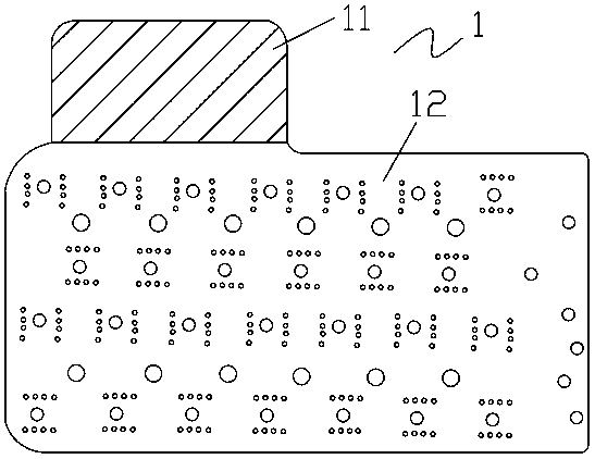
[0023] like figure 1 As shown, a method for manufacturing an inner layer copper plate exposed copper of a power battery circuit board includes the following specific steps:
[0024] S1. According to the customer's requirements, select a copper plate with a thickness of 1.5mm as the inner layer, process the copper plate, drill holes, and contour the copper plate, and use this copper plate as the inner layer plate 1. Wherein the inner layer board is composed of exposed copper area 11 and covering area 12; said exposed copper area is the area where metal copper is exposed after the finished circuit board is made, while the covering area is made into the cost circuit board and covered by the outer layer circuit board covered area.
[0025] S2. Surface treatme...
PUM
Property
Measurement
Unit
thickness
aaaaa
aaaaa
width
aaaaa
aaaaa
Abstract
A method for manufacturing a power cell circuit board while exposing copper of an internal copper plate comprises the following steps: S1, making an internal plate consisting of a copper exposure region (11) and a coverage region (12); S2, performing surface treatment; S3, pasting a high temperature adhesive tape on the copper exposure region (11); S4, covering the whole surface of the internal plate with a layer of prepreg; S5, covering the internal plate with an external circuit board, and performing lamination, drilling, desmearing, full-plate electroplating, pattern transferring, pattern electroplating, circuit etching, solder mask screen printing and profile forming; S6, cutting, by a laser machine, along a connection portion between the copper exposure region (11) and the coverage region (12) of the internal plate; and S7, removing the prepreg layer and the high temperature adhesive tape layer on the surface of the circuit board of the internal plate, to obtain the power cell circuit board. By means of the method, the prepreg in the copper exposure region (11) in the internal plate is effectively removed, so that no adhesive stain is left on the copper exposure region (11), and prepreg residues are avoided; the quality of the circuit board is improved; moreover, the method is suitable for proofing or batch production, so that the production costs are reduced, the production period is shortened, and the production efficiency is improved.
Description
technical field [0001] The invention belongs to the field of circuit board production, and in particular relates to a method for producing exposed copper on an inner layer copper plate of a power battery circuit board. Background technique [0002] With the continuous development of the circuit board industry, circuit boards for various purposes also appear. At present, in addition to the traditional pursuit of precision and fineness, in recent years, due to international and domestic concerns about environmental protection issues, the rapid development of the new energy electric vehicle and motor vehicle industry has been stimulated, and the corresponding demand for circuit boards for high-current and high-voltage battery protection has also been obtained. rapid growth. [0003] Since the power battery circuit board needs to carry large current and high voltage, ordinary circuit boards can no longer meet this requirement. It is necessary to embed a certain thickness of cop...
Claims
Application Information
Patent Timeline
Application Date:The date an application was filed.
Publication Date:The date a patent or application was officially published.
First Publication Date:The earliest publication date of a patent with the same application number.
Issue Date:Publication date of the patent grant document.
PCT Entry Date:The Entry date of PCT National Phase.
Estimated Expiry Date:The statutory expiry date of a patent right according to the Patent Law, and it is the longest term of protection that the patent right can achieve without the termination of the patent right due to other reasons(Term extension factor has been taken into account ).
Invalid Date:Actual expiry date is based on effective date or publication date of legal transaction data of invalid patent.