Electromagnetic wave shielding composite film
An electromagnetic wave and composite film technology, applied in the direction of magnetic/electric field shielding, electrical components, etc., can solve the problems of ineffective shielding of low-frequency electromagnetic waves, high equipment investment costs, etc., and achieve the goal of improving electromagnetic wave shielding effect, light weight, and simplifying the integration process Effect
- Summary
- Abstract
- Description
- Claims
- Application Information
AI Technical Summary
Problems solved by technology
Method used
Image
Examples
Embodiment 1
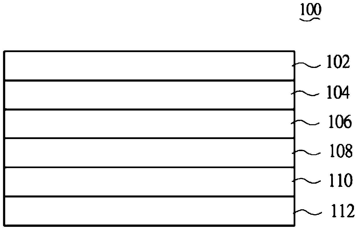
[0029] The electromagnetic shielding composite film of this embodiment is completed by the following process steps: graphene is prepared by mechanical exfoliation, and its average thickness range can be from 0.2 nanometers to 300 nanometers, and then graphene (25% by weight), Low-viscosity macromolecular binder (40 weight percent epoxy resin), hardener (15 weight percent polyamide hardener), dispersant (0.5 weight percent anionic dispersant), organic solvent (19 weight percent butyl Mixed solvent of ketone, toluene and ethyl acetate) and additives (0.5% by weight defoamer) etc. are fully and uniformly mixed, and coated and dispersed on the surface of PET release film 112 to form incident light with high conductive function layer 110, the thickness of which is about 15 microns; then, a wave-absorbing layer 108 of nickel-chromium alloy with a thickness of 50 nm and a reflective layer 106 of copper metal with a thickness of 300 nm are sequentially formed on the surface of the inci...
Embodiment 2
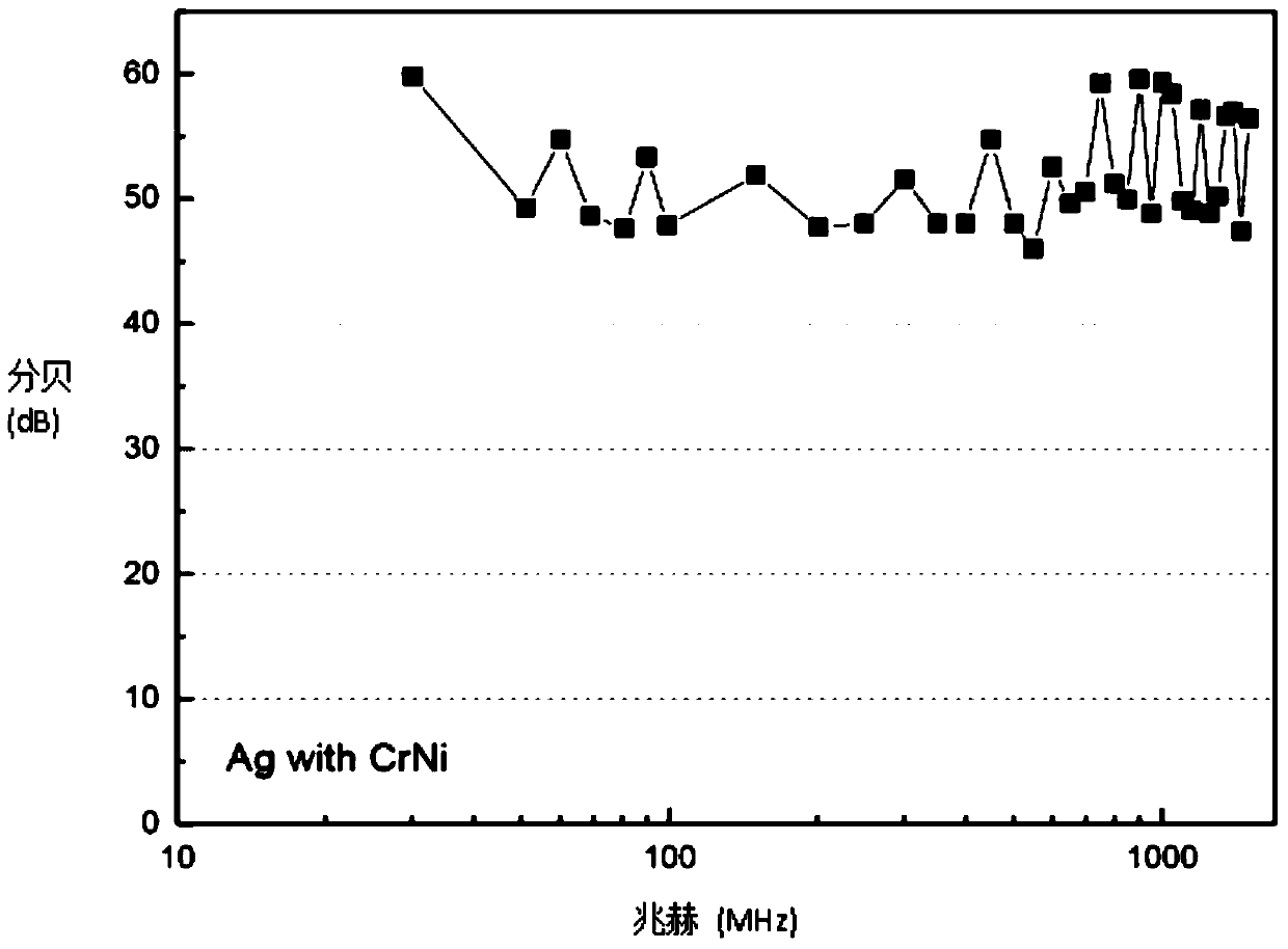
[0031] The electromagnetic shielding composite film of this embodiment is completed by the following process steps: graphene is prepared by mechanical exfoliation, and its average thickness range can be from 0.2 nanometers to 300 nanometers, and then graphene (25% by weight) and Low-viscosity macromolecular binder (40 weight percent epoxy resin), hardener (15 weight percent polyamide hardener), dispersant (0.5 weight percent anionic dispersant), organic solvent (19 weight percent butyl Mixed solvent of ketone, toluene and ethyl acetate) and additives (0.5% by weight defoamer) etc. are fully and uniformly mixed, and coated and dispersed on the surface of PET release film 112 to form incident light with high conductive function layer 110, the thickness of which is about 15 microns; then, a wave-absorbing layer 108 of nickel-chromium alloy with a thickness of 50 nanometers and a reflective layer 106 of silver metal with a thickness of 200 nanometers are sequentially formed on the ...
Embodiment 3
[0033] The electromagnetic shielding composite film of this embodiment is completed by the following process steps: graphene is prepared by mechanical exfoliation, and its average thickness range can be from 0.2 nanometers to 300 nanometers, and then graphene (25% by weight) and Low-viscosity macromolecular binder (40 weight percent epoxy resin), hardener (15 weight percent polyamide hardener), dispersant (0.5 weight percent anionic dispersant), organic solvent (19 weight percent butyl Mixed solvent of ketone, toluene and ethyl acetate) and additives (0.5 weight percent defoamer) etc. are fully and evenly mixed and coated and dispersed on the surface of PET release film 112 to form an incident layer 110 with high conductive function, Its thickness is about 15 microns; then, a wave-absorbing layer 108 of nickel-chromium alloy with a thickness of 50 nanometers and a reflective layer 106 of aluminum metal with a thickness of 300 nanometers are sequentially formed on the surface of...
PUM
| Property | Measurement | Unit |
|---|---|---|
| thickness | aaaaa | aaaaa |
| thickness | aaaaa | aaaaa |
| thickness | aaaaa | aaaaa |
Abstract
Description
Claims
Application Information
 - Generate Ideas
- Intellectual Property
- Life Sciences
- Materials
- Tech Scout
- Unparalleled Data Quality
- Higher Quality Content
- 60% Fewer Hallucinations
Browse by: Latest US Patents, China's latest patents, Technical Efficacy Thesaurus, Application Domain, Technology Topic, Popular Technical Reports.
© 2025 PatSnap. All rights reserved.Legal|Privacy policy|Modern Slavery Act Transparency Statement|Sitemap|About US| Contact US: help@patsnap.com


