Anisotropic conductive film and semiconductor device using same

An anisotropic, conductive film technology, applied to semiconductor devices, electric solid devices, conductive layers on insulating carriers, etc., can solve the problems of reducing composition flow, undisclosed adjustment of anisotropic conductive film of insulating particles, etc., to achieve Effect of Improving Connection Characteristics

Active Publication Date: 2018-03-06
KUKDO ADVANCED MATERIALS CO LTD
View PDF7 Cites 0 Cited by
  • Summary
  • Abstract
  • Description
  • Claims
  • Application Information

AI Technical Summary

Problems solved by technology

[0005] Therefore, as a prior art for adjusting the fluidity of a layer containing conductive particles, in Korean Laid-Open Patent No. 10-2012-0122943, the weights of film-forming resin and radical polymerizable resin are adjusted, and in Korean Laid-Open Patent No. In No. 10-2011-0063586, the thickness of the layer is adjusted, thereby reducing the flow of the composition. However, no ultra-low fluidity anisotropic conductive film for adjusting the content of insulating particles is disclosed.

Method used


Image

  • Anisotropic conductive film and semiconductor device using same
  • Anisotropic conductive film and semiconductor device using same
  • Anisotropic conductive film and semiconductor device using same

Examples


Embodiment 1

[0136] Preparation of Conductive Layer Composition

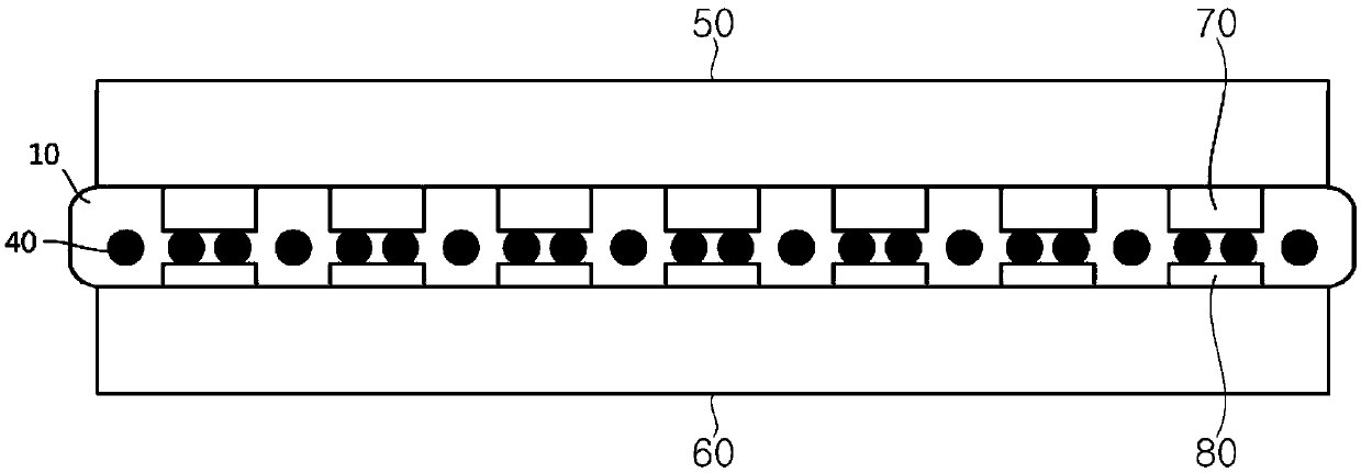
[0137] As the binder resin that functions as a matrix for forming a film, 20 parts by weight of a phenoxy resin (PKHH, Inchemrez company, U.S.) dissolved in a xylene / ethyl acetate azeotrope mixed solvent by 40% by volume, as The curing agent that carries out curing reaction then uses 15 parts by weight of propylene oxide series epoxy resin (EP-4000S, Adeka company, Japan), 10 parts by weight of propylene oxide series epoxy resin (EP-4010S, Adeka company, Japan), Use (Si-60L, Sanshin Chemical, Japan) 5 parts by weight as a thermosetting cationic curing agent, use 30 parts by weight as insulating particles for adding fluidity and insulation (SFP-20M, DENKA, Japan), and use conductive particles ( AUL-704, average particle diameter 4 μm, SEKISUI company, Japan) 20 parts by weight, insulation treatment was performed and mixed to prepare a conductive layer composition.

[0138] Preparation of insulating layer composition

[...

Embodiment 2

[0147] The anisotropic conductive film of Example 2 was produced by the same method and conditions as in Example 1 except that the content of each composition was adjusted as shown in the above-mentioned Table 1 in Example 1.

Embodiment 3

[0149] In Example 1, the anisotropic conductive film of Example 3 was produced by the same method and conditions as in Example 1 except that the content of each composition was adjusted as shown in Table 1 above.


PUM

PropertyMeasurementUnit
electrical resistanceaaaaaaaaaa
thicknessaaaaaaaaaa

Abstract

The present invention relates to an anisotropic conductive film and a semiconductor device connected by the same, which can prevent short circuits and improve cost savings by adjusting the density of conductive particles in an electrode portion crimped between electrodes and the density of conductive particles in a space portion Effects and connection properties.

Description

technical field [0001] The present invention relates to an anisotropic conductive film and a semiconductor device using the same. Background technique [0002] Anisotropic conductive film (Anisotropic conductive film, ACF) refers to the dispersion of conductive particles such as metal particles such as nickel (Ni) or gold (Au) or polymer particles of the above-mentioned metals on resin such as epoxy resin. The formed film-shaped adhesive film means a polymer film having electrical anisotropy and adhesiveness having conductivity in the thickness direction of the film and insulation in the plane direction. [0003] After the anisotropic conductive film is placed between the circuits, the thermocompression bonding process is carried out under specified conditions, and the electrodes of the circuits are electrically connected by conductive particles, forming a space between the electrodes. It is filled with insulating adhesive resin and the conductive particles are independent ...

Claims


Application Information

Patent Timeline
Patent Type & Authority Patents(China)
IPC IPC(8): H01B5/14
CPCH01L24/29H01L24/32H01L24/83H01L2224/2929H01L2224/293H01L2224/29386H01L2224/29499H01L2224/83851H01L2224/83986H01L2924/15788
Inventor 黃慈英金智软朴憬修郑光珍
Owner KUKDO ADVANCED MATERIALS CO LTD
Why Eureka
Try Eureka