Graphene based surface plasmon polariton electric-absorption light modulator

A technology of surface plasmon and optical modulators, which is applied in the fields of instruments, optics, nonlinear optics, etc., can solve the problems of slow modulation rate and low modulation depth, and achieve the effect of increasing modulation depth, reducing relative area, and improving modulation effect

Active Publication Date: 2016-06-22
ZHEJIANG UNIV
View PDF5 Cites 12 Cited by
  • Summary
  • Abstract
  • Description
  • Claims
  • Application Information

AI Technical Summary

Problems solved by technology

However, the modulation rate that can be realized by the current related modulator structure is still very slow, and the modulation depth is low. These problems make it difficult for this type of optical modulator to meet the needs of optoelectronic integrated systems.

Method used


Image

  • Graphene based surface plasmon polariton electric-absorption light modulator
  • Graphene based surface plasmon polariton electric-absorption light modulator
  • Graphene based surface plasmon polariton electric-absorption light modulator

Examples


Embodiment 1

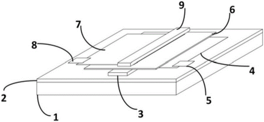
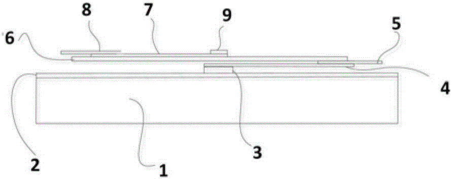
[0037] Such as Figure 1a and Figure 1bThe electroabsorption optical modulator with the structure shown includes: a silicon-based substrate 1, a silicon oxide layer 2, a semiconductor nanoribbon waveguide 3, a single-layer graphene 4, a lower electrode 5, an aluminum oxide dielectric layer 6, and a single-layer graphene 7 , electrode 8 and metal silver waveguide 9. Wherein, the semiconductor nanoribbon waveguide 3 is placed on a silicon-based substrate 1 with a silicon oxide layer 2 of a certain thickness. A single layer of graphene 4 is transferred to the semiconductor nanoribbon waveguide 3, and the graphene on one side is removed by ion beam etching technology. Then on the graphene layer, the lower electrode 5 is prepared by photolithography. Next, thermal evaporation or magnetron sputtering is used to plate an aluminum oxide dielectric layer 6 with a thickness of 10 nm to 100 nm, and the plated dielectric layer cannot completely cover the lower electrode. After the coa...

Embodiment 2

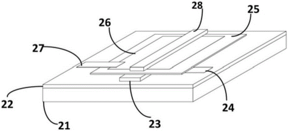
[0039] Such as Figure 2a and Figure 2b The electroabsorption optical modulator of the shown structure includes: a silicon-based substrate 21, a silicon oxide layer 22, a semiconductor nanoribbon waveguide 23, a lower electrode 24, an aluminum oxide dielectric layer 25, a single-layer graphene 26, an electrode 27 and metallic silver waveguide 28.

[0040] Compared with Embodiment 1, in order to reduce the requirements of the manufacturing process, the lower layer of graphene is no longer placed, and the lower electrode 24 is directly connected to the lower semiconductor nanoribbon waveguide 23 by means of photolithography. At the same time, this structure can no longer use the ion beam etching technology to etch the upper single-layer graphene 26 .

Embodiment 3

[0042] Such as Figure 3a and Figure 3b The electroabsorption optical modulator of the structure shown includes: a silicon-based substrate 31, a silicon oxide layer 32, a metal waveguide 33, a single-layer graphene 34, a lower electrode 35, an aluminum oxide dielectric layer 36, a single-layer graphene 37, an electrode 38 and metal waveguide 39.

[0043] Compared with Embodiment 1, both the upper and lower waveguides are made of metal. This structure is designed to generate SPP waves at both the upper and lower interfaces, and the metal acts as a mirror at the interface, which has a better reflection effect, but the non-modulated absorption loss of the metal will be greater. The metal waveguide 33 is placed on the silicon-based substrate 31 with a certain thickness of the oxide layer 32, and the single-layer graphene 34 is placed on the metal waveguide by transfer, and the graphite on the redundant side is removed by ion beam etching and other means alkene. Afterwards, an...


PUM

PropertyMeasurementUnit
widthaaaaaaaaaa
thicknessaaaaaaaaaa
thicknessaaaaaaaaaa

Abstract

The invention discloses a graphene based surface plasmon polariton electric-absorption light modulator.The graphene based surface plasmon polariton electric-absorption light modulator comprises a substrate, a first micro-nano waveguide, a second micro-nano waveguide, a dielectric layer, first single-layer graphene, a first electrode and a second electrode, wherein the first micro-nano waveguide and the second micro-nano waveguide are stacked on the substrate, the dielectric layer and the first single-layer graphene are located between the first micro-nano waveguide and the second micro-nano waveguide, and the first electrode and the second electrode are respectively connected with the first micro-nano waveguide and the second micro-nano waveguide and are used for exerting modulation voltage.At least one of the first micro-nano waveguide and the second micro-nano waveguide is a metal waveguide.The first single-layer graphene is located between one metal waveguide and the dielectric layer.One of the electrodes is connected with the corresponding metal waveguide through the first single-layer graphene.The graphene based surface plasmon polariton electric-absorption light modulator adopts the structural design of vertical arrangement, integrates with the advantages of the graphene and SPP and enables the modulation height to be higher than the height of an existing electric-absorption light modulator and to reach 70% or above.In addition, the light modulator is smaller in structural capacitance, and the overall response speed of the light modulator is greatly improved.

Description

technical field [0001] The invention relates to the application of graphene and surface plasmon polaritons (SPP) in micro-nano optoelectronic systems, in particular to a graphene-based surface plasmon polariton electroabsorption optical modulator. Background technique [0002] As one of the most important devices in modern optoelectronic communication systems, optical modulators can realize fast and accurate coding and modulation of signals. Exploring high-speed, broadband, and compact optical modulators is the goal and direction of research in this field. [0003] As a new type of two-dimensional layered material, graphene has the advantages of strong interaction with graphene, wide operating bandwidth and high-speed operation, and is expected to meet the requirements of high-speed, broadband and compact structure of optical modulators. The surface plasmon effect can realize the strong confinement of the light field, and can realize the operation of the light field on a sm...

Claims


Application Information

Patent Timeline
Patent Type & Authority Applications(China)
IPC IPC(8): G02F1/17
CPCG02F1/17
Inventor 杨青鲁航文庞陈雷徐鹏飞刘旭
Owner ZHEJIANG UNIV
Why Eureka
Try Eureka