Double-waveband composite broadband wave absorbing material based on frequency selective surface

A frequency-selective surface and wave-absorbing material technology, applied to electrical components, magnetic/electric field shielding, antennas, etc., can solve problems such as insufficient bandwidth, achieve widened bandwidth, enhanced wave-absorbing effect, and good wave-absorbing effect

Inactive Publication Date: 2016-06-08
XIDIAN UNIV +1
View PDF4 Cites 15 Cited by
  • Summary
  • Abstract
  • Description
  • Claims
  • Application Information

AI Technical Summary

Problems solved by technology

[0006] The purpose of the present invention is to overcome the deficiencies in the above-mentioned prior art, and propose a dual-band composite broadband absorbing material based on a frequency selective surface, which is used to solve the problem that the bandwidth of the existing absorbing material is not wide enough in the low frequency band, and realize the absorption Waveband bandwidth covers C and X bands

Method used


Image

  • Double-waveband composite broadband wave absorbing material based on frequency selective surface
  • Double-waveband composite broadband wave absorbing material based on frequency selective surface
  • Double-waveband composite broadband wave absorbing material based on frequency selective surface

Examples


Embodiment 1

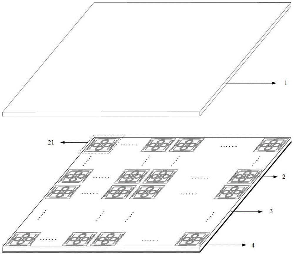
[0023] refer to figure 1 , a dual-band composite broadband absorbing material based on a frequency selective surface, including a base material layer 1, a frequency selective surface 2, a dielectric plate 3 and a floor 4; the base material layer 1 is a rectangular plate of 31.5mm×31.5mm×1.2mm, Its relative permittivity ε'=20.30, relative permeability μ'=3.55, electric loss tangent tanδ D =0.2266, magnetic loss tangent tanδ M =0.4422; the frequency selective surface 2 is a square array formed by 21 periodic arrangements of 7×7 passive resonant units, and the array period is 4.5mm; the dielectric plate 3 is a 31.5mm×31.5mm×1.3mm FR4 rectangular plate; the frequency The selection surface 2 and the floor 4 are printed on the upper and lower surfaces of the dielectric board 3 respectively, and the matrix material layer 1 is glued to the upper surface of the frequency selection surface.

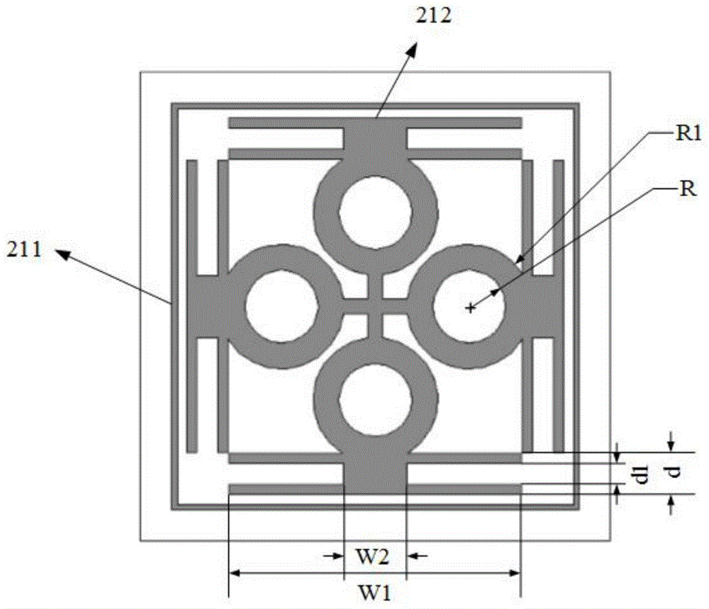
[0024] refer to figure 2 , the passive resonant unit 21 is composed of a square ring patch ...

Embodiment 2

[0025] The structure of embodiment 2 is identical with the structure of embodiment 1, and following parameter has been adjusted:

[0026] The inner diameter R of the four rings in the deformed Jerusalem cross-shaped patch 212 is 0.3 mm, and the outer diameter R1 is 0.6 mm; the arrangement period of the passive resonant unit 21 is 4.4 mm; the base material layer 1 is 30.8 mm×30.8 mm× 1.1mm rectangular plate, its relative permittivity ε'=18.50, relative permeability μ'=3.70, electric loss tangent tanδ D =0.23, magnetic loss tangent tanδ M =0.45; the size of the dielectric board 3 is 30.8mm×30.8mm×1.2mm.

Embodiment 3

[0027] The structure of embodiment 3 is identical with the structure of embodiment 1, and following parameter has been adjusted:

[0028] The inner diameter R of the four rings in the deformed Jerusalem cross-shaped patch 212 is R=0.5mm, and the outer diameter R1=0.8mm; the arrangement period of the passive resonant unit 21 is 4.6mm; the base material layer 1 is 32.2mm×32.2mm× 1.3mm rectangular plate, its relative permittivity ε'=22.00, relative permeability μ'=4.00, electric loss tangent tanδ D =0.25, magnetic loss tangent tanδ M =0.30; the size of the dielectric board 3 is 32.2mm×32.2mm×1.1mm.

[0029] Effect of the present invention can be further illustrated in conjunction with the following simulation results:

[0030] 1. Simulation content

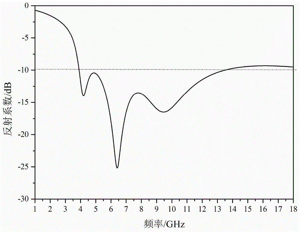
[0031] 1.1 Utilize commercial emulation software HFSS_13.0 to the S of above-mentioned embodiment 1 11 The parameters are simulated and calculated, and the results are as follows image 3 shown.

[0032] 1.2 Utilize the commercia...


PUM

PropertyMeasurementUnit
relative permittivityaaaaaaaaaa

Abstract

The invention discloses a double-waveband composite broadband wave absorbing material based on a frequency selection surface and aims at solving a problem that a bandwidth of an existing wave absorbing material in a low frequency band is not wide enough. The material comprises a matrix material layer, the frequency selection surface, a dielectric plate and a floor. The frequency selection surface and the floor are printed on upper and lower surfaces of the dielectric plate respectively. The matrix material layer and the dielectric plate form an up-down stack structure. The frequency selection surface is formed through periodically arranging M*N passive resonance units, wherein the M is greater than or equal to 3 and the N is greater than or equal to 3. Each passive resonance unit is formed by a square ring paster and a deformed Jerusalem cross type paster located in an internal portion, and central points of the two are superposed. The deformed Jerusalem cross type paster is formed by a middle cross, four circular rings which are located on a middle cross axis and are successively connected to the middle cross axis and four I-shaped structures. The material possesses advantages that an absorption frequency band is wide and a wave absorbing characteristic is high. Absorption and shielding of electromagnetic waves in C and X wave bands can be realized. The material can be used for fields of communication, environmental protection, human body protection and the like.

Description

technical field [0001] The invention belongs to the technical field of frequency-selective surfaces in wave-absorbing materials, and relates to a dual-band composite broadband wave-absorbing material based on a frequency-selective surface. The material absorbs a wide frequency band and has strong wave-absorbing characteristics, and can be used for communication, environmental protection and human body protection and many other fields. Background technique [0002] With the rapid development of science, there are more and more technologies and various products using electromagnetic waves as the medium, and the impact of electromagnetic radiation on the environment is also increasing. For example, radio waves may cause interference to the airport environment, causing aircraft flights to fail to take off normally and be delayed; mobile phone signals may interfere with the work of various precision electronic medical devices; computers will radiate electromagnetic waves carrying...

Claims


Application Information

Patent Timeline
Patent Type & Authority Applications(China)
IPC IPC(8): H01Q17/00H05K9/00
Inventor 姜文龙毛龚书喜张帅洪涛李时良
Owner XIDIAN UNIV
Why Eureka
Try Eureka