
Frit contact membrane layer and OLED packaging structure with frit contact membrane layer

A technology of packaging structure and glass frit, which is applied in the direction of semiconductor devices, electrical components, circuits, etc., can solve the problems affecting the packaging strength and water and oxygen barrier ability, so as to enhance the packaging strength, enhance the ability to block water and oxygen, and increase contact area effect

Inactive Publication Date: 2016-05-11
KUNSHAN GO VISIONOX OPTO ELECTRONICS CO LTD
View PDF10 Cites 12 Cited by
  • Summary
  • Abstract
  • Description
  • Claims
  • Application Information

AI Technical Summary

Problems solved by technology

[0004] When glass frit is packaged, the glass frit will inevitably be in contact with the film layer on the substrate. The structure of the part of the glass frit in contact with the film layer on the substrate will affect the packaging strength on the one hand, and affect the water and oxygen barrier capacity on the other hand.

Method used


Image

  • Frit contact membrane layer and OLED packaging structure with frit contact membrane layer
  • Frit contact membrane layer and OLED packaging structure with frit contact membrane layer
  • Frit contact membrane layer and OLED packaging structure with frit contact membrane layer

Examples


Embodiment Construction

[0019] In order to further illustrate the technical means and functions adopted by the present invention to achieve the intended purpose of the invention, the present invention will be described in detail below in conjunction with the accompanying drawings and preferred embodiments.

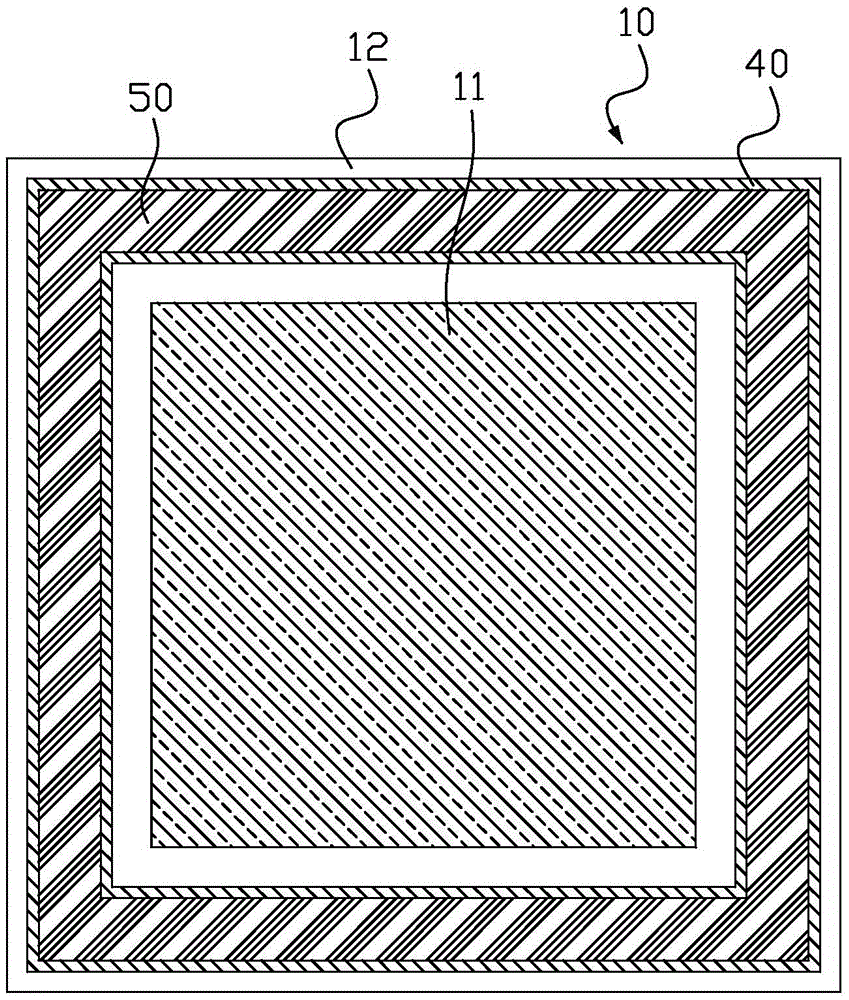
[0020] figure 1 Shown is a schematic cross-sectional view of the OLED packaging structure provided by the present invention. figure 2 Shown is a schematic top view of the OLED packaging structure provided by the present invention. Such as figure 1 and figure 2 As shown, the OLED packaging structure of the present invention includes a glass substrate 10, a packaging cover plate 20, an OLED element 30 on the glass substrate 10, a glass frit contact film layer 40, and a glass between the glass substrate 10 and the packaging cover plate 20. Material 50.

[0021] further reference figure 2 , the glass substrate 10 is a rectangular structure, which includes a rectangular display area 11 and a r...


PUM


Abstract

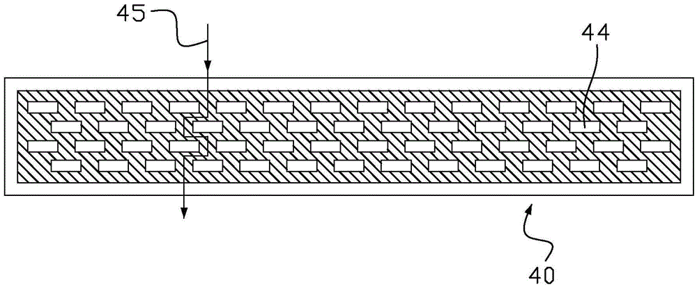
The invention provides a frit contact membrane layer and an OLED packaging structure with the frit contact membrane layer. The OLED packaging structure comprises a glass substrate, the frit contact membrane layer and a frit, wherein the frit contact membrane layer is positioned on the glass substrate; the frit is in contact with the frit contact membrane layer; the frit contact membrane layer is provided with a plurality of openings in an area corresponding to a frit coating area; the openings are arranged at intervals and arranged into a plurality of rows along the extension direction of the frit; corresponding openings in the adjacent rows are mutually staggered; one part of the frit fills the openings; and one part of the frit is in contact with the upper surface of the frit contact membrane layer. According to the OLED packaging structure disclosed by the invention, the mutually staggered openings are formed in the frit contact membrane layer; therefore, the contact area between the frit and the frit contact membrane layer is increased; the OLED packaging strength is increased; furthermore, a channel for water and oxygen to enter can also be extended through the mutually staggered openings; and the water and oxygen obstructing capability of the frit can be improved.

Description

technical field [0001] The invention relates to the technical field of OLED encapsulation, in particular to a glass frit contact film layer and an OLED encapsulation structure thereof. Background technique [0002] In recent years, OLED (Organic Light-Emitting Diode, organic electroluminescent display) has entered the public eye as an emerging flat-panel display because of its good color contrast, active light emission, wide viewing angle, thinning, fast response speed and low energy consumption. And other advantages, it is recognized as one of the most promising display technology that can replace LCD. However, in OLED displays, organic light-emitting layers and electrodes are prone to failure when exposed to water and oxygen, thus greatly affecting the service life of OLED devices. Therefore, various materials are used in the industry to seal the OLED device in the glass casing, so as to isolate the organic light-emitting layer and the electrode from the surrounding envir...

Claims


Application Information

Patent Timeline
Patent Type & Authority Applications(China)
IPC IPC(8): H01L51/52
CPCH10K50/8426
Inventor 彭兆基张伸福
Owner KUNSHAN GO VISIONOX OPTO ELECTRONICS CO LTD
Learn More