Manufacturing method of semiconductor device and semiconductor device manufactured by method

A device manufacturing method and semiconductor technology, which are applied in the fields of semiconductor/solid-state device manufacturing, semiconductor devices, electrical components, etc., can solve the problems of complex superjunction semiconductor processes, and achieve cost-effective, widened application fields, and enhanced current conduction capabilities. Effect

Inactive Publication Date: 2016-04-27
FUJIAN FUXIN ELECTRONICS TECH CO LTD
View PDF5 Cites 2 Cited by
  • Summary
  • Abstract
  • Description
  • Claims
  • Application Information

AI Technical Summary

Problems solved by technology

[0003] The technical problem to be solved by the present invention is to provide a semiconductor device manufacturing method and a semiconductor device manufactured by the method, so as to solve the complicated problem of the existing super junction semiconductor process

Method used


Image

  • Manufacturing method of semiconductor device and semiconductor device manufactured by method
  • Manufacturing method of semiconductor device and semiconductor device manufactured by method
  • Manufacturing method of semiconductor device and semiconductor device manufactured by method

Examples


Embodiment Construction

[0032] In order to describe the technical content, structural features, achieved goals and effects of the present invention in detail, the following will be described in detail in conjunction with the embodiments and accompanying drawings.

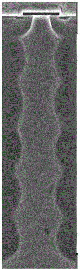
[0033] see figure 1 , figure 2 , Figure 3a-Figure 3g as well as Figure 4 , the present invention provides a semiconductor device manufacturing method, comprising the following steps: as Figure 3a As shown, in the first step, a layer of N-type epitaxial layer ② is grown on an N-type substrate ①, that is, a layer of N-type epitaxial layer ② is stacked on an N-type substrate ①. In the second step, an intrinsic epitaxial layer③ is grown on the N-type epitaxial layer, such as Figure 3b As shown, a layer of intrinsic epitaxial layer ③ is stacked on the N-type epitaxial layer. The third step is to implant N-type impurities on the intrinsic epitaxial layer, such as Figure 3c shown. The fourth step is to implant P-type impurities at a ...


PUM


Abstract

The invention provides a manufacturing method of a semiconductor device and the semiconductor device manufactured by the method. The method comprises the following steps: (1) growing an N-type epitaxial layer on an N-type substrate; (2) growing an intrinsic epitaxial layer on the N-type epitaxial layer; (3) injecting N-type impurities into the intrinsic epitaxial layer; (4) injecting P-type impurities into the preset position of the intrinsic epitaxial layer; (5) repeating the steps (2) to (4); (6) carrying out thermal annealing; and (7) injecting a P-type well into the preset position. According to the manufacturing method, the process difficulty and the cost are reduced; meanwhile, the performance is not obviously weakened; and the cost performance is relatively high.

Description

technical field [0001] The invention relates to the field of semiconductor device manufacturing, in particular to a method for manufacturing a semiconductor device and a semiconductor device manufactured by the method. Background technique [0002] The traditional structure of VDMOS (Vertical Double Diffused Metal-Oxide Semiconductor Field Effect Transistor), with the increase of breakdown voltage, because the doping concentration of the epitaxial layer is relatively low and the thickness is relatively large, the on-resistance will be very large, which It is commonly referred to as "SiLimit". For high-voltage devices, in order to reduce the on-resistance or break through the SiLimit, the current mainstream technology is to use super-junction technology. At present, there are two development paths for super junction technology. One is to form a super junction on an N+ substrate through multiple N-type epitaxial growth and P-type implantation, but the process cost is relative...

Claims


Application Information

Patent Timeline
Patent Type & Authority Applications(China)
IPC IPC(8): H01L21/336H01L29/06H01L29/78
CPCH01L29/66712H01L29/0615H01L29/7802
Inventor 孙晓儒陈虞平王熹伟刘海波胡兴正
Owner FUJIAN FUXIN ELECTRONICS TECH CO LTD
Why Eureka
Try Eureka