Junction barrier Schottky diode with gradient depth P type region and preparation method thereof

A junction barrier Schottky and diode technology, applied in diodes, semiconductor/solid-state device manufacturing, electrical components, etc., can solve the problem of easy reverse breakdown of diodes, achieve good ohmic contact, enhance breakdown performance, improve performance effect

Pending Publication Date: 2021-03-19
CHANGCHUN INST OF OPTICS FINE MECHANICS & PHYSICS CHINESE ACAD OF SCI
View PDF6 Cites 1 Cited by
  • Summary
  • Abstract
  • Description
  • Claims
  • Application Information

AI Technical Summary

Problems solved by technology

[0005] Based on this, it is necessary to provide a junction barrier Schottky diode with a gradient depth P-type region and a preparation method for the problem that the existing junction barrier Schottky diode is easy to reverse breakdown

Method used


Image

  • Junction barrier Schottky diode with gradient depth P type region and preparation method thereof
  • Junction barrier Schottky diode with gradient depth P type region and preparation method thereof
  • Junction barrier Schottky diode with gradient depth P type region and preparation method thereof

Examples


Embodiment Construction

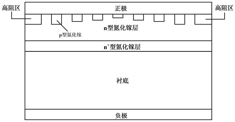
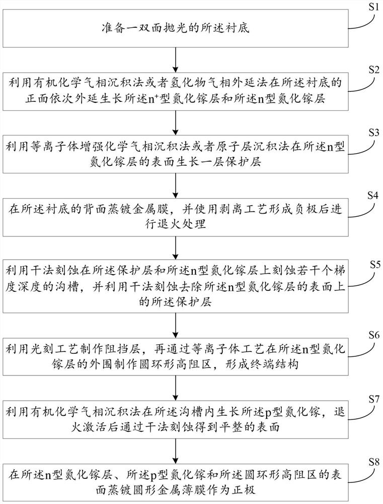
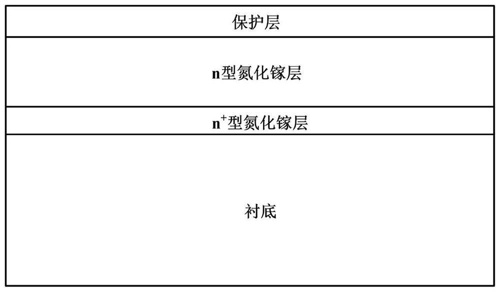
[0031] The main purpose of the present invention is to provide a new structure and a new method for enhancing the reverse breakdown and leakage current characteristics of gallium nitride (GaN)-based junction barrier Schottky diode (JBS) devices from the perspective of device structure and technology. The preparation method of the structure can obtain a high-performance GaN-based junction barrier Schottky diode through a relatively simple process, which provides a new way for the further development and application of the junction barrier Schottky diode. Among them, JBS mainly includes the following structures: GaN-based metal-semiconductor-metal structure, Schottky structure, P-N structure and PIN structure. The present invention uses the terminal structure and the structure of increasing the gradient depth p-type region on the Schottky diode to improve the reverse breakdown characteristics and leakage current characteristics of the device. The contact part conducts, and the P...


PUM

PropertyMeasurementUnit
thicknessaaaaaaaaaa
thicknessaaaaaaaaaa
thicknessaaaaaaaaaa

Abstract

The invention relates to a junction barrier Schottky diode with a gradient depth P type region and a preparation method thereof. The junction barrier Schottky diode comprises: a substrate; a negativeelectrode, which is manufactured on the back surface of the substrate; an n+ type gallium nitride layer, which epitaxially grows on the front surface of the substrate; an n type gallium nitride layer,which epitaxially grows on the n+ type gallium nitride layer, wherein an annular high-resistance region is arranged on the periphery of the n type gallium nitride layer, a plurality of grooves with gradient depths are etched in the n type gallium nitride layer, and p type gallium nitride grows in each groove; and a positive electrode, which is manufactured on the surfaces of the n type gallium nitride layer, the p type gallium nitride layer and the annular high-resistance region. The P type region with the gradient depth can adjust the electric field distribution of the high-electric-field-intensity region of the device; meanwhile, good ohmic contact and better PN junctions can be formed through the double-layer epitaxial gallium nitride structure, and the performance of the device is effectively improved; and in addition, the high-resistance region can effectively restrain breakdown of the device located on the edge of the electrode under high voltage, and the breakdown performance of the device is enhanced.

Description

technical field [0001] The invention relates to the technical field of semiconductors, in particular to a gallium nitride-based junction barrier Schottky diode and a preparation method thereof. Background technique [0002] In recent years, due to the low turn-on voltage drop and extremely short reverse recovery time of the Schottky Barrier Diode (SBD), the improvement of the efficiency of the circuit system has attracted people's attention and has been widely used. SBD has three outstanding features: (1) The turn-on voltage and conduction voltage drop of SBD are smaller than that of PIN diodes, which can effectively reduce the power loss in the circuit; (2) SBD has a lower junction capacitance, and its operating frequency is as high as 100GHz (3) Since there is no injection of minority carriers, the switching speed of SBD is faster, and its own reverse recovery time is only the charging and discharging time of the Schottky barrier capacitance. The traditional Schottky diod...

Claims


Application Information

Patent Timeline
Patent Type & Authority Applications(China)
IPC IPC(8): H01L29/06H01L29/872H01L21/329
CPCH01L29/0607H01L29/0684H01L29/66212H01L29/872
Inventor 黎大兵刘新科孙晓娟贾玉萍石芝铭
Owner CHANGCHUN INST OF OPTICS FINE MECHANICS & PHYSICS CHINESE ACAD OF SCI
Why Eureka
Try Eureka