Semiconductor manufacturing process control system and analysis method

A production process and control system technology, applied in semiconductor/solid-state device manufacturing, electrical components, circuits, etc., can solve problems such as yield rate of fragmented products, omissions in sorting and analysis, and problems with etching machine parameters

Inactive Publication Date: 2016-04-06
SEMICON MFG INT (SHANGHAI) CORP
View PDF3 Cites 7 Cited by
  • Summary
  • Abstract
  • Description
  • Claims
  • Application Information

AI Technical Summary

Problems solved by technology

For example, although when checking the etching depth of wafer products, the data is within the range specified by the upper and lower limits every time, but as the etching depth increases, there may be problems with the parameters of the etching machine, so the next etching data may exceed the standard , in this case, the next etching data must wait until it is checked and found to exceed the standard before generating an alarm
At the same time, at present, the generalization and data analysis of data exceeding the standard trend is usually done manually by engineers. Due to the complicated workload and huge amount of data, it is very likely that there will be omissions during the sorting and analysis, resulting in fragmentation or product yield reduction.

Method used


Image

  • Semiconductor manufacturing process control system and analysis method
  • Semiconductor manufacturing process control system and analysis method
  • Semiconductor manufacturing process control system and analysis method

Examples


Embodiment Construction

[0076] The present invention will be further described below in conjunction with the accompanying drawings and specific embodiments, but not as a limitation of the present invention.

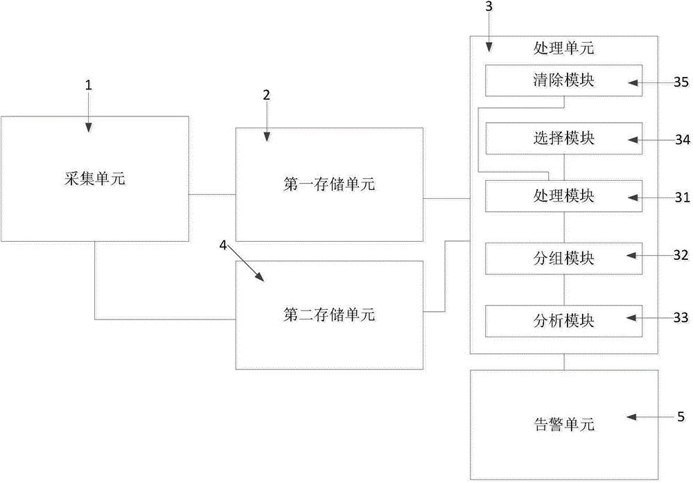
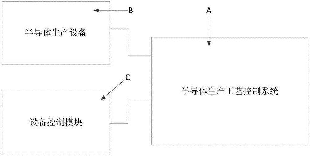
[0077] like figure 1 As shown, in a preferred embodiment of the present invention, a semiconductor production process control system is suitable for statistical process control of semiconductor production, and further, can be used for process control of wafers on semiconductor production equipment; The semiconductor production process control system specifically includes:

[0078] The collection unit 1 is used to collect raw wafer data generated by semiconductor production equipment.

[0079] The first storage unit 2 is connected to the acquisition unit 1; the acquisition unit 1 saves the collected wafer raw data in the first storage unit 2. In a preferred embodiment of the present invention, the raw wafer data in the first storage unit 2 is stored in the time sequence in which the correspondi...


PUM


Abstract

The invention discloses a manufacturing process control system and an analysis method, which belong to the technical field of semiconductor manufacturing process management and control. The semiconductor manufacturing process control system comprises an acquisition unit, a first storage unit, a processing unit and an alarm unit, wherein the acquisition unit acquires wafer original data; the first storage unit stores the wafer original data; the processing unit extracts the wafer original data and processes the wafer original data to obtain multiple groups of grouped data, and analyzes and outputs a variation trend of the grouped data; and the alarm unit receives an analysis result and outputs an alarm signal. The analysis method comprises the steps of: acquiring the wafer original data and storing the wafer original data in the first storage unit; extracting the wafer original data from the first storage unit, and processing the wafer original data to obtain the corresponding grouped data and dividing the grouped data into groups; and analyzing the variation trend of the grouped data, and outputting the analysis result to the alarm unit for alarm. The semiconductor manufacturing process control system and the analysis method have the beneficial effects of reducing alarm time delay and omission, avoiding fragment risk of products, and ensuring product yield.

Description

technical field [0001] The invention relates to the technical field of semiconductor process management and control, in particular to a semiconductor production process control system and analysis method. Background technique [0002] In the manufacturing process of semiconductor integrated circuits, data measurement, data collection, and data monitoring are all important reasons that directly affect the yield of semiconductor products. Specifically, in the production process of semiconductors, especially wafers, statistical process control technology (Statistical Process Control, SPC) needs to be used. The so-called SPC is a process control tool with the help of mathematical statistics. It analyzes and evaluates the production process, discovers the symptoms of systemic factors in time according to the feedback information, and takes measures to eliminate their influence, so that the process can be maintained in a controlled state only affected by random factors, so as to ...

Claims


Application Information

Patent Timeline
IPC IPC(8): H01L21/67
Inventor 姚海燕杨旭东暨欣媛张昊
Owner SEMICON MFG INT (SHANGHAI) CORP
Why Eureka
Try Eureka