Preparation of crosslinked electrode modification materials by adopting an olefinic bond-thiol group click chemistry method and applications of the materials in organic electronic devices
An electrode modification and chemical method technology, applied in the field of polymer optoelectronic materials and devices, can solve the problems of high energy consumption, pollution and high raw material cost, and achieve the effects of improving work function, good resistance to solvent elution, and improving device performance.
- Summary
- Abstract
- Description
- Claims
- Application Information
AI Technical Summary
Problems solved by technology
Method used
Image
Examples
Embodiment 1
[0040] The synthetic route of the representative cross-linkable conjugated polymer PFN-V containing ethylenic groups in the side chain is as follows:
[0041]
[0042] (1) Preparation of monomer 2
[0043] Add 6.48g (20mmol) dibromofluorene and 540mg (0.22mmol) tetrabutylammonium bromide in a 250mL three-necked flask with a stirring bar, add 75mL toluene solution and 75mL mass fraction of 50% sodium hydroxide solution, After stirring for 5 minutes, 90mL (50mmol) 6-bromo-1-hexene was slowly added dropwise, and the reaction was refluxed for 17h. The reaction solution was extracted with water and ethyl acetate, the organic layer was dried with anhydrous magnesium sulfate, and suction filtered. After the obtained filtrate was rotary evaporated, it was passed through a column with petroleum ether as the eluent, and the final product was white crystals. 1 HNMR (500MHz, CDCl3, δ, ppm): 7.52‐7.48 (d, 2H), 7.47‐7.41 (d, 4Hz), 5.66‐5.56 (m, 2H), 4.89‐4.81 (t, 4H, J=18Hz) ,1.96‐1.89...
Embodiment 2
[0050] Taking the polymer PFN-V as an example to illustrate that this kind of polymer has the performance of anti-solvent elution after cross-linking treatment
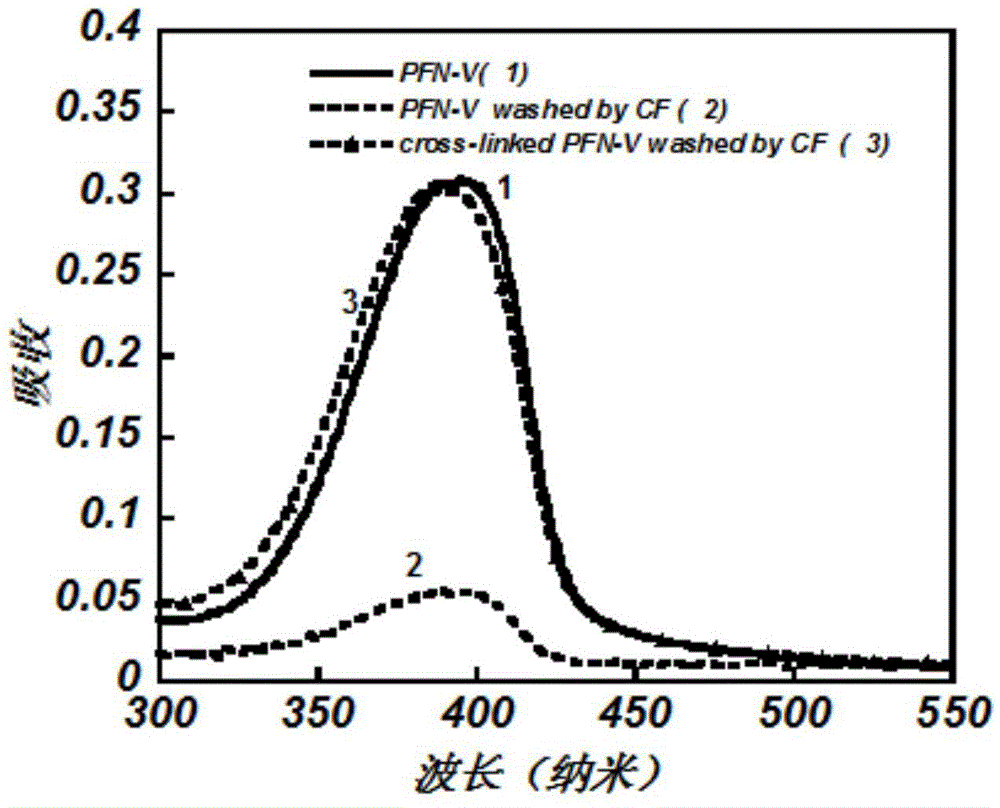
[0051] The polymer PFN-V synthesized in Example 1 was dissolved in chloroform, then 77% of 1,8-octanedithiol was added, the solution was filtered with a 0.45 micron filter membrane, and spin-coated on a quartz plate to form a film with a thickness of about 20 nanometers. Measure the absorbance of PFN‐V after film formation with a UV tester (HP8453spectrophotometer) produced by Hewlett-Packard Company, corresponding to figure 2 Curve 1. Afterwards, the PFN-V film is irradiated with ultraviolet light with a wavelength of 365 nm to form an insoluble cross-linked film. The cross-linked PFN-V film was soaked in chloroform pure solvent.
[0052] The absorbance of the cross-linked PFN-V after being washed with chloroform was measured by UV test, corresponding to figure 2 Curve 3 in, from which we can see the crosslinki...
Embodiment 3
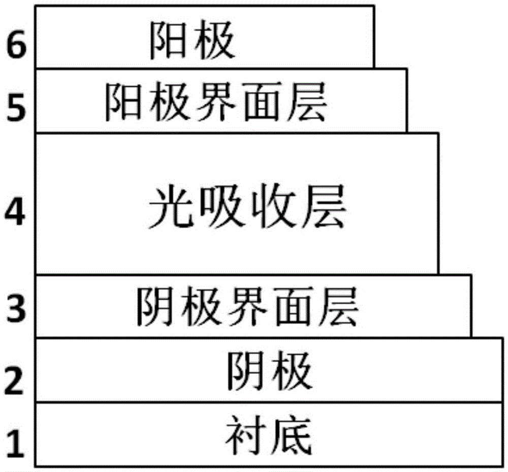
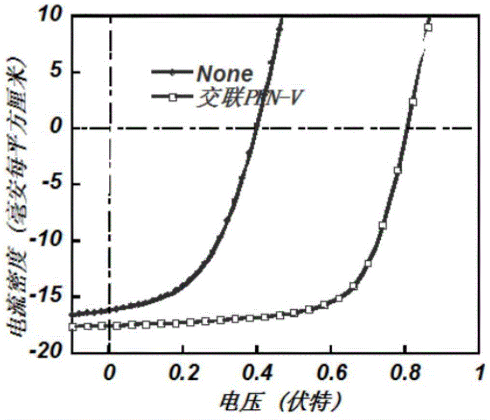
[0054] The cross-linked conjugated polymer PFN-V synthesized in Example 2 is used as a cathode interface modification in an inverted organic solar cell (ITO cathode / cathode interface layer / active layer / anode-machine interface layer / anode)
[0055] Pre-cut the ITO conductive glass with a square resistance of 20 ohms / cm2 into 15mm×15mm square pieces. Use acetone, special detergent for micron-sized semiconductors, deionized water, and isopropanol to clean ultrasonically in sequence, blow nitrogen whistle, and place in a constant temperature oven for later use. Take a chloroform solution of conjugated polymer PFN‐V and 1,8‐octanedithiol (mass ratio 1:0.77), and spin-coat it on ITO with a thickness of about 8 nm. The films were then irradiated under UV light for 5 seconds to complete the cross-linking. Then spin-coat the active layer material PTB7‐Th:PC 71 BM (mass ratio 1:1.5), with a thickness of 100 nm, and finally vapor-deposited MoO3 and Al electrodes. All preparations were...
PUM
 Abstract
Description
Claims
Application Information
 - Generate Ideas
- Intellectual Property
- Life Sciences
- Materials
- Tech Scout
- Unparalleled Data Quality
- Higher Quality Content
- 60% Fewer Hallucinations
Browse by: Latest US Patents, China's latest patents, Technical Efficacy Thesaurus, Application Domain, Technology Topic, Popular Technical Reports.
© 2025 PatSnap. All rights reserved.Legal|Privacy policy|Modern Slavery Act Transparency Statement|Sitemap|About US| Contact US: help@patsnap.com


