
Substrate installation platform, plasma processing device, and operation method for plasma processing device

A technology for mounting platforms and processing devices, used in the manufacture of discharge tubes, electrical components, semiconductor/solid-state devices, etc., and can solve problems such as failure, substrate processing effect is different from the central area, damage to electrostatic chucks, etc.

Active Publication Date: 2016-03-30
ADVANCED MICRO FAB EQUIP INC CHINA
View PDF4 Cites 3 Cited by
  • Summary
  • Abstract
  • Description
  • Claims
  • Application Information

AI Technical Summary

Problems solved by technology

This creates a pronounced temperature gradient on the edge of the substrate, resulting in a significantly different substrate treatment around the edge than in the center
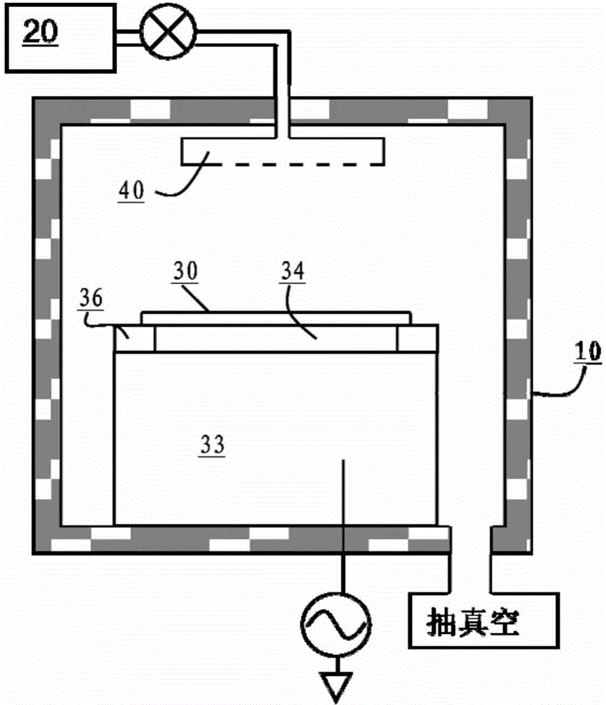
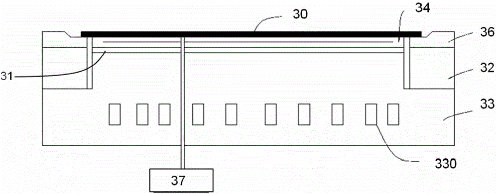
The gap between the electrostatic chuck 34 and the focus ring 36 will form a channel, and part of the plasma will reach the bottom of the substrate along the channel to corrode the side of the electrostatic chuck and the organic adhesive layer 31 between the electrostatic chuck 34 and the base 33, which in turn can damage the electrostatic chuck or even render it useless

Method used


Image

  • Substrate installation platform, plasma processing device, and operation method for plasma processing device
  • Substrate installation platform, plasma processing device, and operation method for plasma processing device
  • Substrate installation platform, plasma processing device, and operation method for plasma processing device

Examples


Embodiment Construction

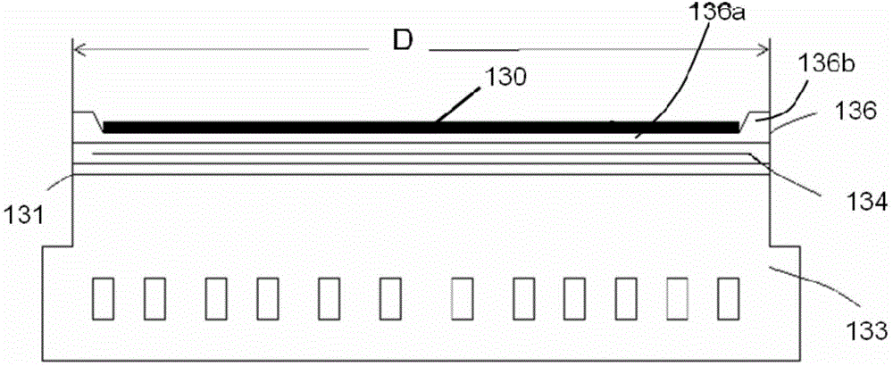
[0018] The present invention aims to solve the inhomogeneity of temperature in different regions of the substrate during the plasma treatment process, and at the same time prevent the side wall of the electrostatic chuck 34 on the back of the substrate from being corroded. An electrostatic chuck provides temperature control of the tray. Such as image 3 Shown is the first embodiment of the present invention, an adhesive layer 131 is included above the base 133 , an electrostatic chuck 134 is included above the adhesive layer 131 , and a tray 136 of the present invention is fixed above the electrostatic chuck. The tray 136 of the present invention includes a flat plate portion 136a and a raised portion 136b, wherein the raised portion 136b and the flat plate portion 136a are made of insulating materials such as SiO2, Al2O3, AlN, etc., and the upper surface of the raised portion 136b is on the main body material of the insulating material A layer of semiconductor material such ...


PUM


Abstract

The invention relates to a substrate installation platform, a plasma processing device, and an operation method for the plasma processing device. The device comprises a reaction cavity, and the lower part of the interior of the reaction cavity comprises a conductive substrate, a static chuck, a pallet, and a substrate. The static chuck is fixed on the conductive substrate, and the pallet is placed on the static chuck. The substrate is fixed in the pallet, and the pallet comprises a panel part and an upwards bulged part, wherein the diameter of the upper surface of the panel part is greater than the diameter of the substrate. The bulged part surrounds the panel part and the substrate on the panel part. The diameter of the static chuck is greater than the diameter of the substrate, and is less than or equal to the diameter of the pallet.

Description

technical field [0001] The invention relates to the technical field of semiconductor manufacturing, in particular to a substrate support plate in a plasma processing device and an operating method thereof. Background technique [0002] Such as figure 1 As shown, the plasma processing device includes a reaction chamber 10, the reaction chamber includes a base 33, and the base includes a lower electrode. Above the susceptor is an electrostatic chuck 34 on which the substrate 30 to be processed is placed, and a focus ring 36 surrounds the electrostatic chuck. A radio frequency power supply 35 with a lower frequency (such as 2Mhz-400Khz) is connected to the lower electrode 33 in the base through a matcher. The top of the reaction chamber also includes a gas distribution device 40, such as a gas shower head, or a nozzle for passing the reaction gas into the reaction chamber. The gas distribution device is connected to a gas source 20 through a flow diverter or switching valve....

Claims


Application Information

Patent Timeline
IPC IPC(8): H01J37/20H01J37/32H01L21/683
Inventor 左涛涛吴狄倪图强
Owner ADVANCED MICRO FAB EQUIP INC CHINA
Learn More