Method and system for brittle fracturing of brittle semiconductor materials

A semiconductor and brittle technology, applied in welding equipment, laser welding equipment, metal processing equipment, etc., can solve the problems of reduced bending strength of brittle semiconductor materials, affecting the use of brittle semiconductor materials, and low cutting efficiency, etc., to improve the efficiency of splitting, Elimination of micro-cracks and stress concentration, uniform heating effect

Active Publication Date: 2017-12-12
WUHAN EXCEL SCI & TECH LTD EST
View PDF8 Cites 0 Cited by
  • Summary
  • Abstract
  • Description
  • Claims
  • Application Information

AI Technical Summary

Problems solved by technology

[0003] For brittle semiconductor materials, taking silicon wafer cutting as an example, the mainstream cutting technology still uses diamond blade cutting. This cutting method has disadvantages such as wide cutting slit width, low cutting efficiency, and high cost of consumables. Therefore, laser cutting wafers should become the mainstream. technology, but because laser cutting textures or laser cutting marks are left when laser cutting silicon wafers, there are actually a lot of micro-cracks and stress concentration hidden under these marks, and they also have a certain roughness. As time goes by, These cracks gradually spread to the middle of the circuit of the chip, causing the chip to be scrapped
In engineering, a three-point test or a four-point test method is used to measure whether and how much the flexural strength of the brittle material after cutting is reduced after the brittle material is cut by laser. The general laser cutting method causes the existence of many microcracks due to the cutting texture. , leading to a sharp decrease in the bending strength of brittle semiconductor materials after laser cutting, which affects the subsequent use of brittle semiconductor materials

Method used


Image

  • Method and system for brittle fracturing of brittle semiconductor materials
  • Method and system for brittle fracturing of brittle semiconductor materials
  • Method and system for brittle fracturing of brittle semiconductor materials

Examples


Embodiment 1

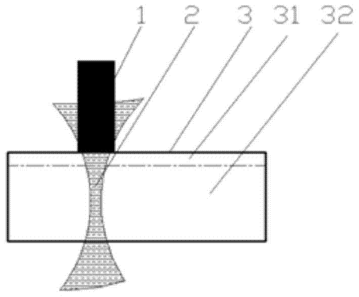
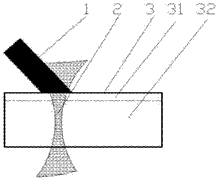
[0042] Embodiment 1. A method for brittle fracturing of brittle semiconductor materials. The following combination Figure 1-a to Figure 2-b The method provided in this embodiment will be described in detail.

[0043] see Figure 1-a and Figure 1-b As shown, the method provided in this embodiment includes: using a heating laser beam to rapidly heat the inside of the brittle semiconductor material to be split, so that the internal expansion of the brittle semiconductor material to be split forms a compressive stress, and at the same time, the brittle semiconductor material to be split The surface of the part is cooled rapidly, so that the surface of the part to be split of the brittle semiconductor material shrinks to form tensile stress, so that the brittle semiconductor material undergoes brittle fracture and a smooth cut is formed. Wherein, the brittle semiconductor material is optically transparent or partially optically transparent to the heating laser beam, so that the...

Embodiment 2

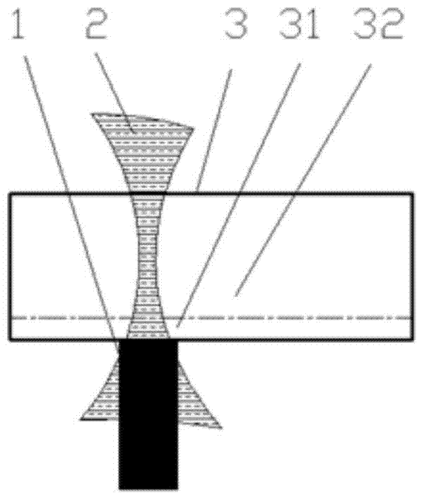
[0055] Embodiment 2. A brittle fracture system of brittle semiconductor materials. The following combination Figure 3-a and Figure 3-b The system provided by this embodiment is described.

[0056] see Figure 3-a As shown, the system provided by this embodiment includes a heating module and a cooling module, wherein the heating module uses a heating laser beam 2 to rapidly heat the inside 32 of the brittle semiconductor material 3 to be split, so that the brittle semiconductor material 3 to be split The internal 3 expands to form compressive stress; at the same time, the cooling module rapidly cools the surface 31 of the brittle semiconductor material 3 to be split, so that the surface 31 of the brittle semiconductor material 3 to be split shrinks to form tensile stress, so that the brittle semiconductor material 3 A brittle fracture occurs to form a smooth cut; wherein, the brittle semiconductor material 3 is optically transparent or partially optically transparent to th...


PUM

PropertyMeasurementUnit
wavelengthaaaaaaaaaa

Abstract

The invention discloses a method and system for brittle fracturing of brittle semiconductor materials. The method includes: using a heating laser beam to rapidly heat the inside of the brittle semiconductor material to be cleaved, so that the inside of the brittle semiconductor material to be cleaved expands to form a pressure At the same time, the surface of the brittle semiconductor material to be split is rapidly cooled, so that the surface of the brittle semiconductor material to be split shrinks to form tensile stress, so that the brittle semiconductor material undergoes brittle fracture and forms a smooth incision. Through the present invention, the brittle semiconductor material can be processed perfectly, and compared with the traditional brittle semiconductor material processing method, it can obtain extremely high incision quality, maintain the bending strength of the brittle semiconductor material, and improve the brittle semiconductor material. Fragmentation efficiency.

Description

technical field [0001] The invention relates to the technical field of laser processing, in particular to a method and system for brittle fracturing of brittle semiconductor materials. Background technique [0002] The difference between brittle fracture and ductile fracture is mainly divided from the macroscopic characteristics, and the judgment basis is "whether there is obvious plastic deformation before fracture". Brittle fracture hardly produces plastic deformation before fracture. It is generally stipulated that when the reduction of area of ​​a smooth tensile specimen is less than 5%, it belongs to brittle fracture. The fracture is flat and bright, with metallic luster, and perpendicular to the normal stress. In ductile fracture, significant plastic deformation occurs before fracture, and with plastic deformation and energy absorption, the shape of the workpiece is necked, bent, and the section shrinks. [0003] For brittle semiconductor materials, taking silicon waf...

Claims


Application Information

Patent Timeline
Patent Type & Authority Patents(China)
IPC IPC(8): B23K26/38B23K26/402B23K26/70
CPCB23K26/38
Inventor 张立国
Owner WUHAN EXCEL SCI & TECH LTD EST
Why Eureka
Try Eureka