Slow wave structure of coplanar waveguide

A technology of slow wave structure and coplanar waveguide, which is applied in traveling wave tubes, circuit components of transit time tubes, discharge tubes, etc., can solve problems such as difficult to achieve high characteristic impedance and difficult grounding, and achieve miniaturization and integration, low operating voltage, and small parasitic parameters

Inactive Publication Date: 2016-03-23
UNIV OF ELECTRONICS SCI & TECH OF CHINA
View PDF8 Cites 11 Cited by
  • Summary
  • Abstract
  • Description
  • Claims
  • Application Information

AI Technical Summary

Problems solved by technology

Microstrip lines are widely used, but there are still two obvious disadvantages: 1) It is

Method used


Image

  • Slow wave structure of coplanar waveguide
  • Slow wave structure of coplanar waveguide
  • Slow wave structure of coplanar waveguide

Examples


Embodiment

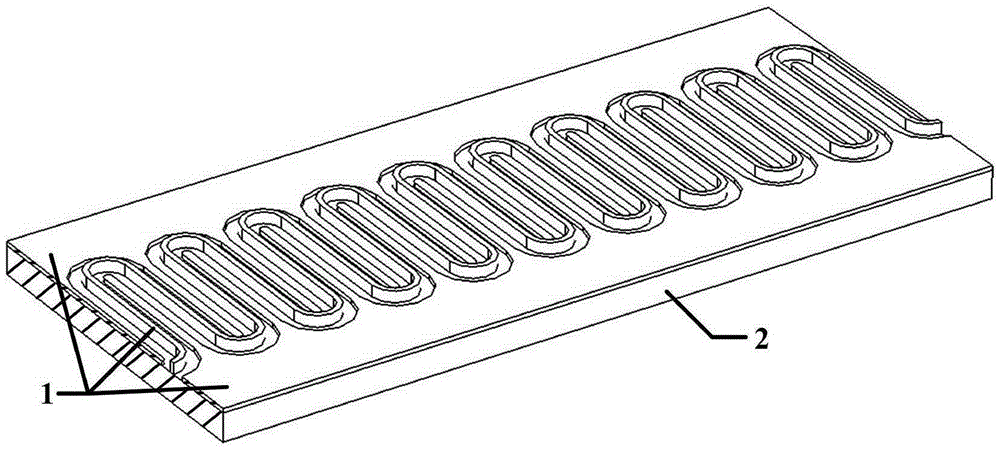
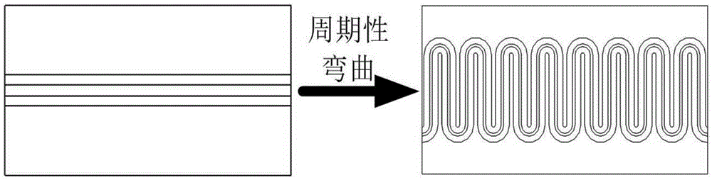
[0027] A slow-wave structure with coplanar waveguides, such as figure 1 As shown, this figure is a schematic structural diagram of a specific embodiment of the present invention, including a metal layer 1 and a dielectric substrate 2. The metal layer 1 is printed on the dielectric substrate 2 using printed circuit technology. The metal layer 1 includes a central conductive strip and grounded metal surfaces located on both sides of the central conductive strip. The shape of the central conductive strip is a periodic bending curve, and the central conductive strip and the grounded metal surfaces on both sides form two parallel narrow grooves.

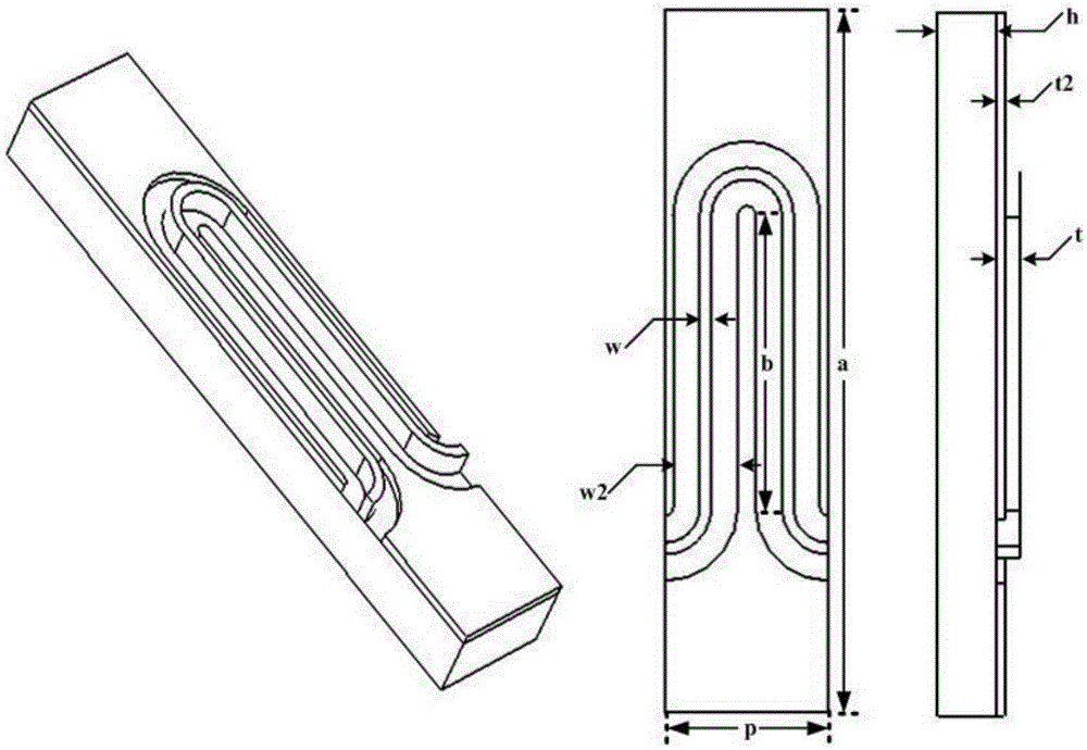
[0028] like figure 2 As shown, the dimensions of the above-mentioned N-shaped curved coplanar waveguide slow-wave structure are defined as follows: the dielectric constant of the dielectric substrate 2 is ε, the thickness of the dielectric substrate is h, the lateral length is a, the period length is p, and the central conduction band wi...


PUM


Abstract

The invention discloses a slow wave structure of a coplanar waveguide, wherein the slow wave structure of the coplanar waveguide belongs to the technical field of microwave electrovacuum and relates to a travelling wave tube amplifier device. The slow wave structure of the coplanar waveguide comprises a dielectric substrate (2) and a metal layer (1) on the surface of the dielectric substrate (2). The metal layer (1) comprises a central conduction band and grounded metal surfaces at two sides of the central conduction band. The shape of the central conduction band is a periodical bent curve. The central conduction band is isolated from the grounded metal surfaces at two sides. The slow wave structure of the coplanar waveguide can effectively settle a problem of electron accumulation on a microstrip slow wave structure, and serial connection or parallel connection with other microwave devices is easily realized, thereby easily realizing small size and integration of a vacuum device. The vacuum device with the structure of the invention has relatively low working voltage, and the coupling impedance curve and the dispersion curve are relatively flat, thereby realizing wide frequency band of the vacuum device and reducing gain fluctuation of the vacuum device in the working frequency band. Therefore the slow wave structure of the coplanar waveguide has relatively high potential and is suitable for a miniature planar travelling wave tube.

Description

technical field [0001] The design of the invention belongs to the field of microwave electric vacuum technology, and relates to a traveling wave tube amplifier. Background technique [0002] Traveling wave tube amplifier is a microwave vacuum device that amplifies high-frequency signals through the energy exchange between electromagnetic field and electron beam. Due to its high power, high gain, high efficiency, broadband and long life, traveling wave tubes play a pivotal role in the field of vacuum electronics and are widely used in electronic countermeasures, communications, guidance and other fields. [0003] At present, helical traveling wave tubes and coupled cavity traveling wave tubes are the most widely used in various fields. Although these two types of traveling wave tubes have the advantages of high power and wide bandwidth, they are bulky and heavy. Compared with solid-state devices , can not meet the urgent needs of modern electronic technology light weight, sm...

Claims


Application Information

Patent Timeline
IPC IPC(8): H01J25/00H01J25/34H01J23/24
CPCH01J23/24H01J25/00H01J25/34
Inventor 丁冲魏彦玉王媛媛张鲁奇李倩郭彍宫玉彬王文祥
Owner UNIV OF ELECTRONICS SCI & TECH OF CHINA
Why Eureka
Try Eureka