
Circuit board surface treatment method

A surface treatment, circuit board technology, applied in secondary treatment of printed circuits, improvement of metal adhesion of insulating substrates, printed circuits, etc. Good quality, good welding performance, and the effect of increasing the bonding force

Active Publication Date: 2016-03-02
GUANGZHOU FASTPRINT CIRCUIT TECH +2
View PDF3 Cites 7 Cited by
  • Summary
  • Abstract
  • Description
  • Claims
  • Application Information

AI Technical Summary

Problems solved by technology

Based on the many advantages of copper-nickel-gold electroplating, it has been widely used by various printed circuit board manufacturers. However, the gold surface of the circuit board processed by conventional electroplating copper-nickel-gold surface is whiter, and even thicker gold plating cannot meet the requirements of the gold surface. Matte gold is required, the surface is smooth and bright gold, which makes the welding wettability poor, which is not conducive to the subsequent welding process, increases the difficulty of welding, and affects product quality

Method used


Image

  • Circuit board surface treatment method

Examples


Embodiment Construction

[0027] Embodiments of the present invention are described in detail below in conjunction with accompanying drawings:

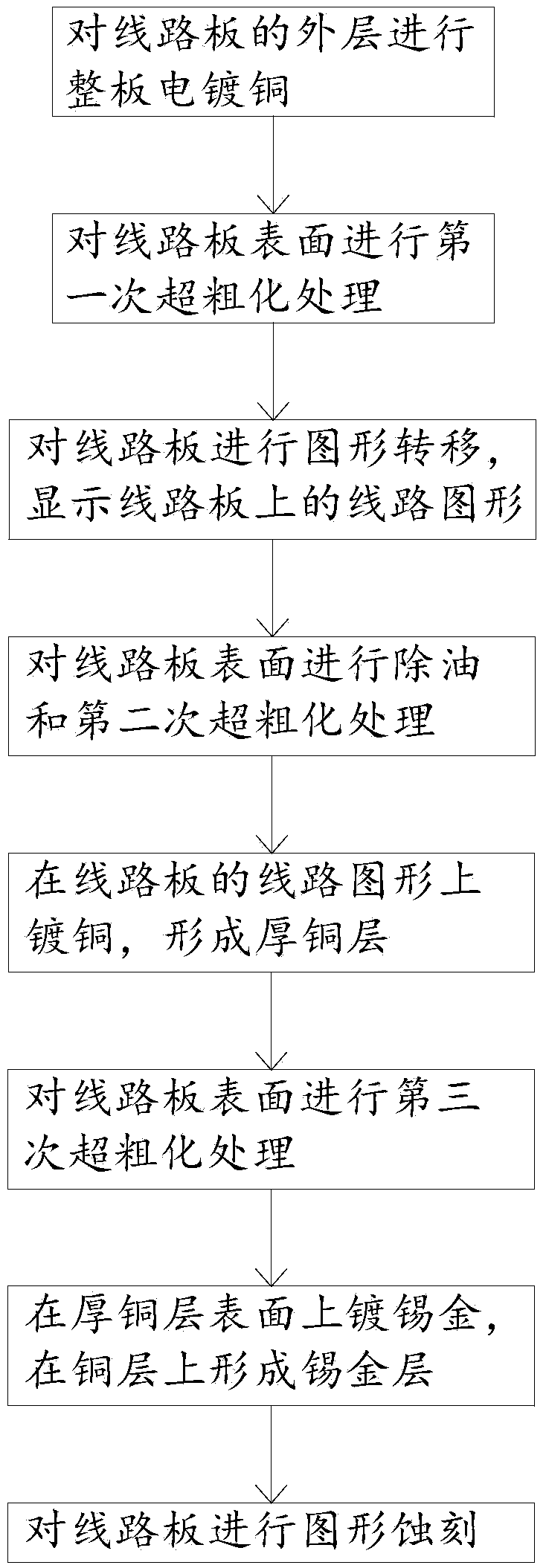
[0028] Such as figure 1 Shown, a kind of surface treatment method of circuit board is characterized in that, comprises the following steps:

[0029] Electroplate copper on the outer layer of the circuit board;

[0030] Perform the first super-roughening treatment on the surface of the circuit board;

[0031] Carry out graphics transfer to the circuit board, and display the circuit graphics on the circuit board;

[0032] Degreasing and second super-roughening treatment on the surface of the circuit board;

[0033] Plating copper on the circuit pattern of the circuit board to form a thick copper layer;

[0034] Perform the third super-roughening treatment on the surface of the circuit board;

[0035] Nickel-gold plating on the surface of the thick copper layer to form a nickel-gold layer on the thick copper layer;

[0036] Pattern etching of circuit boards...


PUM


Abstract

The invention relates to a circuit board surface treatment method. The circuit board surface treatment method comprises the following steps: performing entire-board copper electroplating on the outer layer of the circuit board; performing the first time of super-roughening treatment on the surface of the circuit board; performing pattern transferring on the circuit board and displaying the circuit pattern on the circuit board; performing oil removing and the second time of super-roughening treatment on the surface of the circuit board; plating copper on the circuit pattern of the circuit board to form a thick copper layer; performing the third time of super-roughening treatment on the surface of the circuit board; and plating nickel-gold alloy on the surface of the thick copper layer to form a nickel-gold alloy layer on the thick copper layer. Before the nickel-gold alloy is plated, the copper surface of the circuit board is roughened by the three times of super-roughening treatment; the roughened copper surface enables the gold surface that is plated with the nickel-gold alloy to be dark so as to satisfy the requirement on a matte gold color; the circuit board, after performing the pattern transferring and before performing the nickel-gold alloy plating, is also subjected to two times of super-roughening treatment in order to prevent the circuit copper surface, that is developed after performing the pattern transferring, from being directly electroplated with the nickel-gold alloy in the non-oxidized condition, so that the shortcoming that the copper layer is separated from the nickel-gold alloy layer is avoided.

Description

technical field [0001] The invention relates to the technical field of printed circuit electroplating, in particular to a method for surface treatment of circuit boards. Background technique [0002] In the component welding process of printed circuit boards, the surface treatment quality of printed circuit boards is particularly important. The most basic purpose of surface treatment is to ensure good solderability or electrical properties. Existing in the form of oxides, it is unlikely to remain as virgin copper for long, so other treatments of the copper are required. Electroplating copper-nickel-gold surface treatment process electroplates a thick layer of nickel-gold alloy with good electrical properties on the copper surface, which can protect the printed circuit board for a long time; in addition, it also has environmental protection that other surface treatment processes do not have Patience. Based on the many advantages of copper-nickel-gold electroplating, it has ...

Claims


Application Information

Patent Timeline
Patent Type & Authority Applications(China)
IPC IPC(8): H05K3/38H05K3/24
CPCH05K3/24H05K3/383H05K2203/0392
Inventor 邓敦文李艳国陈蓓
Owner GUANGZHOU FASTPRINT CIRCUIT TECH
Learn More