
Printed light-emitting display without pixel bank and manufacturing method thereof

A technology of a light-emitting display and a manufacturing method, which is applied in the fields of semiconductor/solid-state device manufacturing, semiconductor devices, electric solid-state devices, etc., can solve the problems of complex manufacturing process and high cost, and achieve the advantages of simplifying the manufacturing process, reducing the manufacturing cost, and preventing color crosstalk. Effect

Active Publication Date: 2019-10-11
武汉国创科光电装备有限公司
View PDF5 Cites 0 Cited by
  • Summary
  • Abstract
  • Description
  • Claims
  • Application Information

AI Technical Summary

Problems solved by technology

[0006] In view of the above-mentioned deficiencies in the prior art, the object of the present invention is to provide a printed light-emitting display without pixel banks and its manufacturing method, aiming to solve the problems of complicated manufacturing process and high cost of the existing printed light-emitting display

Method used


Image

  • Printed light-emitting display without pixel bank and manufacturing method thereof
  • Printed light-emitting display without pixel bank and manufacturing method thereof
  • Printed light-emitting display without pixel bank and manufacturing method thereof

Examples


Embodiment Construction

[0028] The present invention provides a printed light-emitting display without pixel banks and its manufacturing method. In order to make the purpose, technical solution and effect of the present invention clearer and clearer, the present invention will be further described in detail below. It should be understood that the specific embodiments described here are only used to explain the present invention, not to limit the present invention.

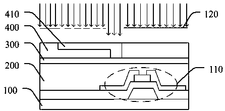
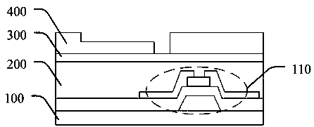
[0029] see figure 1 , figure 1 It is a flow chart of a preferred embodiment of a method for manufacturing a printed light-emitting display without a pixel bank of the present invention, as shown in the figure, which includes steps:

[0030] S1. Make a flat passivation layer on the TFT substrate, then deposit a hydrophobic film layer on the flat passivation layer, and then deposit a photoresist layer on the hydrophobic film layer;

[0031] S2. Expose the photoresist layer through a mask, wherein the area to be made of the pixel electrode...


PUM


Abstract

The invention discloses a printing type light-emitting display without pixel bank and a manufacturing method thereof. The present invention forms the pixel electrode embedded in the hydrophobic thin film layer on the TFT substrate. Since the pixel electrode does not protrude relative to the surface of the hydrophobic thin film layer at this time, the short circuit of the device will not be caused when the light-emitting element is made, so the production of the pixel bank is omitted. At the same time, Since the pixel electrode is embedded in the hydrophobic material, when the printing process is used to prepare the light-emitting element, after the ink is deposited on the pixel electrode, it will form a large contact angle and will not spread to the connected pixel electrode, thereby effectively preventing the contact between adjacent pixels. Mutual cross color.

Description

technical field [0001] The invention relates to the field of display technology, in particular to a printed light-emitting display without pixel banks and a manufacturing method thereof. Background technique [0002] In the contemporary information society, the importance of display devices as a visual information transmission medium is further strengthened. In order to occupy a dominant position in the future, display devices are moving towards lighter, thinner, lower energy consumption, lower cost and better Trends in image quality. [0003] Organic electroluminescent diode (OLED) has the advantages of self-illumination, fast response, wide viewing angle, high brightness, light and thin, etc. Quantum dot light-emitting diode (QLED) has high light color purity, high luminous quantum efficiency, and easy-to-adjust luminous color. These two light-emitting devices are the two main directions of display device research at present. The preparation process of OLED mainly includ...

Claims


Application Information

Patent Timeline
Patent Type & Authority Patents(China)
IPC IPC(8): H01L27/32H01L21/77H01L51/52H01L51/56
CPCH01L21/77H10K59/125H10K50/80H10K2102/302H10K71/00
Inventor 陈亚文
Owner 武汉国创科光电装备有限公司
Learn More