


Quick Research
Generate reliable direction feasibility study reports for your R&D in just a few steps.

Technical Q&A
Discover and master advanced knowledge NOW. Basics, ideas, possibilities, all at once.

Find Solutions
As an expert in R&D theories, this can generate solutions to your technical problems instantly.

Evaluate Feasibility
Analyze your overall solution with one click, know your potential R&D risks in advance.

Monitor Landscape
Get weekly tech updates, stay abreast of the latest tech innovations and key insights.
Chip sealing ring structure and manufacturing method thereof
A manufacturing method and sealing ring technology, which are used in the manufacture of semiconductor/solid-state devices, electrical components, and electrical solid-state devices, etc., can solve the problems of complex structure and low rupture strength, and achieve simple structure, improved yield, and enhanced resistance to The effect of burst strength
- Summary
- Abstract
- Description
- Claims
- Application Information
AI Technical Summary
Problems solved by technology
Method used
Image

Examples
Embodiment 1
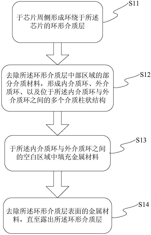
[0044] like image 3 and Figure 4 ~ Figure 7 As shown, the present embodiment provides a method for manufacturing a chip sealing ring structure, including steps:
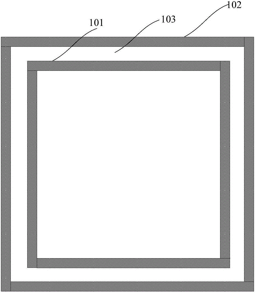
[0045] like image 3 and Figure 4 As shown, step 1) S11 is first performed to form an annular dielectric layer 10 surrounding the chip 20 on the peripheral side of the chip 20 .
[0046] As an example, the material of the annular dielectric layer 10 is silicon dioxide, of course, other dielectric materials such as silicon nitride are also applicable, and are not limited thereto.
[0047] In addition, the shape of the annular dielectric layer 10 depends on the shape of the chip 20. In this embodiment, the shape of the chip 20 is rectangular, and the annular dielectric layer 10 has a rectangular ring structure.
[0048] As an example, the annular dielectric layer 10 can be prepared by chemical vapor deposition and other methods, such as plasma enhanced chemical vapor deposition and the like. In this embodiment,...
Embodiment 2
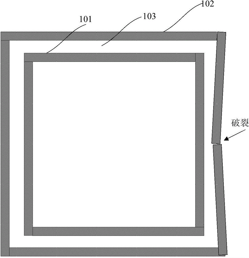
[0074] Such as image 3 and Figure 8 As shown, this embodiment provides a method for manufacturing a chip sealing ring structure, the basic steps of which are as in Embodiment 1, wherein the plurality of dielectric columnar structures 103 between the inner dielectric ring 101 and the outer dielectric ring 102 are in double rows distributed.
[0075] Such as Figure 8 As shown, this embodiment also provides a chip sealing ring structure, the basic structure of which is the same as that of Embodiment 1, wherein a plurality of dielectric columnar structures 103 between the inner dielectric ring 101 and the outer dielectric ring 102 are distributed in double rows.
Embodiment 3
[0077] Such as image 3 and Figure 9 As shown, this embodiment provides a method for manufacturing a chip sealing ring structure, the basic steps of which are as in Embodiment 1, wherein the plurality of dielectric columnar structures 103 between the inner dielectric ring 101 and the outer dielectric ring 102 are in multiple rows distributed.
[0078] Such as Figure 9 As shown, this embodiment also provides a chip sealing ring structure, the basic structure of which is the same as in Embodiment 1, wherein the plurality of dielectric columnar structures 103 between the inner dielectric ring 101 and the outer dielectric ring 102 are distributed in multiple rows.
[0079] As mentioned above, the present invention provides a chip sealing ring structure and a manufacturing method thereof, the manufacturing method comprising the steps of: 1) forming an annular dielectric layer 10 surrounding the chip on the peripheral side of the chip; 2) removing the annular dielectric layer P...
PUM
| Property | Measurement | Unit |
|---|---|---|
| Width | aaaaa | aaaaa |
| Radial size | aaaaa | aaaaa |
| Width | aaaaa | aaaaa |
Abstract
Description
Claims
Application Information
 - R&D Engineer
- R&D Manager
- IP Professional
- Industry Leading Data Capabilities
- Powerful AI technology
- Patent DNA Extraction
Browse by: Latest US Patents, China's latest patents, Technical Efficacy Thesaurus, Application Domain, Technology Topic, Popular Technical Reports.
© 2024 PatSnap. All rights reserved.Legal|Privacy policy|Modern Slavery Act Transparency Statement|Sitemap|About US| Contact US: help@patsnap.com