A kind of photodetector and its preparation method and application
A photodetector and photodetection technology, which is applied in the manufacture/processing of thermoelectric devices and the material of the junction lead wires of thermoelectric devices, can solve the problems of low detection ability of thermal detectors, and achieve a wide range of detection light intensity and integrated Simple, easy-to-integrate effects
- Summary
- Abstract
- Description
- Claims
- Application Information
AI Technical Summary
Problems solved by technology
Method used
Image
Examples
Embodiment 1
[0044] 1) After the glass sheet is ultrasonically rinsed with secondary water, ethanol, acetone, blown dry with nitrogen, and cleaned with plasma, it is soaked in a mixture of n-hexane and octadecyltrichlorosilane with a volume ratio of 100:1. in the solution, take it out after 10 minutes, and obtain a glass sheet with a hydrophobic surface, that is, a substrate;
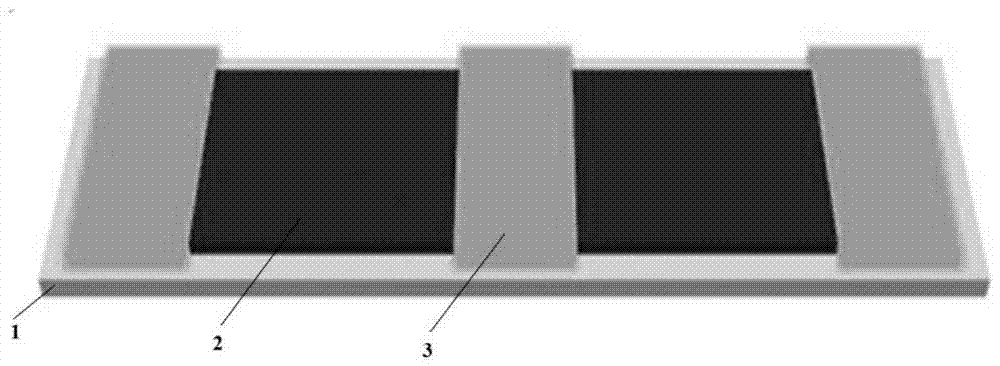
[0045] 2) Utilize n-hexane, absolute ethanol, chloroform to sonicate, rinse, and dry the glass sheet with nitrogen, stick a hollow strip mask, and treat it with a 250-watt ultraviolet ozone cleaning machine for 12 minutes to obtain a hydrophilic strip pattern, the structure will be The active material poly[Cu x (Cu-ett)] or poly[K x (Ni-ett)] (x is 1-2, n is 100-10000, A is Cu or K) is dropped on the glass sheet to form a strip-shaped film, that is, the active layer;
[0046] 3) Place the device obtained in step 2) in a vacuum coating machine at a vacuum degree of 7×10 -6 Under the condition of Pa, on the active ...
Embodiment 2
[0053] Embodiment 2, to the detection of 808 nanometer infrared laser
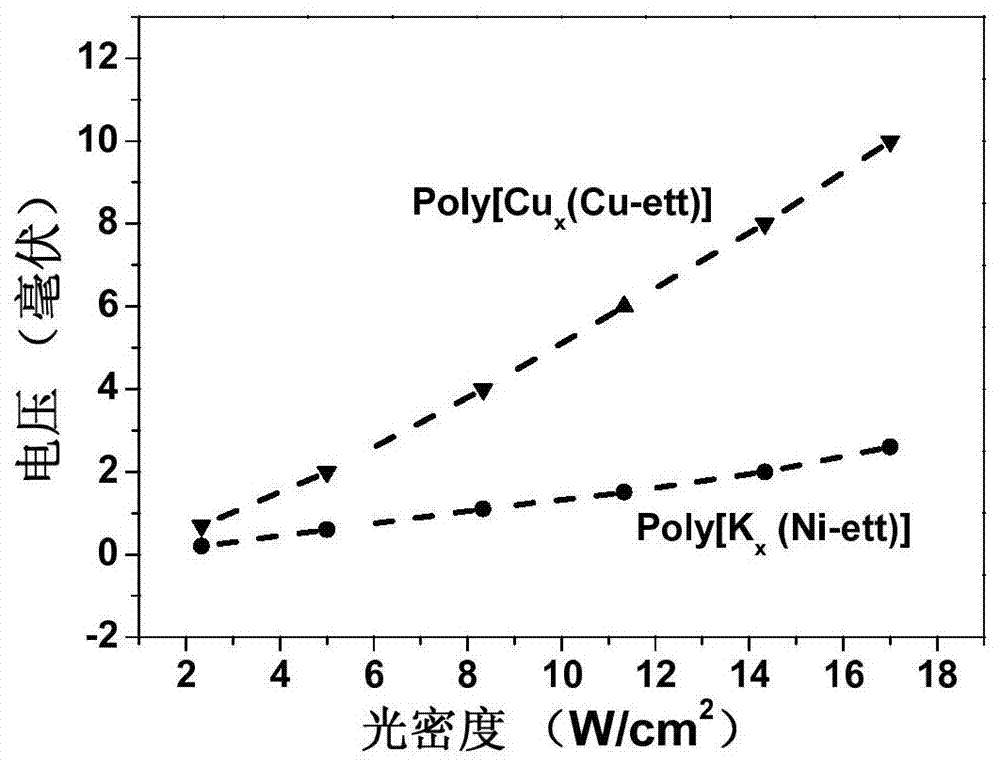
[0054] 1) Utilize the photothermoelectric device obtained in embodiment 1, with poly[Cu x (Cu-ett)] is the relationship between the voltage generated by the detection of the active layer and the optical density of infrared light: when 800 nanometers of infrared light is hit at the interface between the gold electrode and the active layer, the generated voltage is linear with the increase in optical density enhanced ( image 3 ), and for poly[Cu x (Cu-ett)] material, when the optical density reaches 17 W / cm 2 At this time, the generated voltage is as high as 10 millivolts, realizing a large voltage output.
[0055] 2) Utilize the photothermoelectric device obtained in embodiment 1, with poly[K x (Ni-ett)] replacing poly[Cu x (Cu-ett)] is the relationship between the voltage generated by the detection of the active layer and the optical density of infrared light: when 800 nanometers of infrared light is...
Embodiment 3
[0058] 1) After the glass sheet is ultrasonically rinsed with secondary water, ethanol and acetone, blown dry with nitrogen, and cleaned with plasma, it is soaked in a solution with a volume ratio of n-hexane:octadecyltrichlorosilane=100:1 In the process, take it out after 10 minutes to obtain a glass sheet with a hydrophobic surface, that is, a substrate;
[0059] 2) Utilize n-hexane, absolute ethanol, chloroform to sonicate, rinse, and dry the glass sheet with nitrogen, stick a hollow strip mask, and treat it with a 250-watt ultraviolet ozone cleaning machine for 12 minutes to obtain a hydrophilic strip pattern, the structure will be The active material poly[Cu x (Cu-ett)] (x is 1-2, n is 100-10000, A is Cu) drops on the glass sheet to form Figure 5 The thin film in the stripe pattern shown, i.e. the active layer;
[0060] 3) Place the device obtained in step 2) in a vacuum coating machine at a vacuum degree of 7×10 -6 Under the condition of Pa, on the active layer obt...
PUM
 Abstract
Description
Claims
Application Information
 - Generate Ideas
- Intellectual Property
- Life Sciences
- Materials
- Tech Scout
- Unparalleled Data Quality
- Higher Quality Content
- 60% Fewer Hallucinations
Browse by: Latest US Patents, China's latest patents, Technical Efficacy Thesaurus, Application Domain, Technology Topic, Popular Technical Reports.
© 2025 PatSnap. All rights reserved.Legal|Privacy policy|Modern Slavery Act Transparency Statement|Sitemap|About US| Contact US: help@patsnap.com


