Substrate for flexible photoelectronic device, and preparation method thereof
A technology for optoelectronic devices and substrates, which is applied in the fields of electrical solid-state devices, semiconductor/solid-state device manufacturing, and electrical components. and other problems, to achieve the effect of improving light transmittance, improving water and oxygen barrier capacity, and improving performance
- Summary
- Abstract
- Description
- Claims
- Application Information
AI Technical Summary
Problems solved by technology
Method used
Image

Examples
Embodiment 1
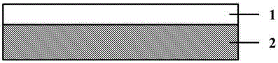
[0043] Such as figure 1 In the substrate structure shown, the flexible substrate 2 is a polyimide film doped with 0.2% cationic UV-sensitive adhesive and 10% aloe vera gel by mass ratio, and the conductive layer 1 is graphene.
[0044] The preparation method is as follows:
[0045] ① Clean the rigid substrate with a surface roughness less than 1nm first, then use detergent, acetone, deionized water, and isopropanol to perform ultrasonic cleaning, and dry it with dry nitrogen after cleaning;
[0046] ② Prepare a mixed film of polyimide, cationic UV-sensitive glue and aloe gel by spin coating on a rigid substrate, the film thickness is 5 μm, and the raw material of the cationic UV-sensitive glue includes the following components:
[0047] Epoxy resin or modified epoxy resin 85%
[0048] Thinner 10%
[0049] Cationic photoinitiator 5%;
[0050] ③ Prepare a conductive layer from graphene aqueous dispersion in ② surface spraying method, the height is 20cm, the spraying pressure...
Embodiment 2
[0056] Such as figure 1 In the substrate structure shown, the flexible substrate 2 is a polyimide film doped with 0.5% cationic UV-sensitive glue and 15% aloe vera gel by mass ratio, and the conductive layer 1 is carbon nanotubes.
[0057] The preparation method is as follows:
[0058] ① Clean the rigid substrate with a surface roughness less than 1nm first, then use detergent, acetone, deionized water, and isopropanol to perform ultrasonic cleaning, and dry it with dry nitrogen after cleaning;
[0059] ② Prepare a mixed film of polyimide, cationic UV-sensitive glue and aloe gel by spin coating on a rigid substrate, the film thickness is 20 μm, and the cationic UV-sensitive glue raw material includes the following components:
[0060] Epoxy resin or modified epoxy resin 87%
[0061] Thinner 9%
[0062] Cationic photoinitiator 4%;
[0063] ③ In ② surface spraying method, the carbon nanotube aqueous dispersion is prepared as a conductive layer, the height is 20cm, the sprayi...
Embodiment 3
[0069] Such as figure 1 In the substrate structure shown, the flexible substrate 2 is a polystyrene film doped with 2% cationic UV-sensitive glue and 23% aloe vera gel by mass ratio, and the conductive layer 1 is silver nanowires.
[0070] The preparation method is as follows:
[0071] ① Clean the rigid substrate with a surface roughness less than 1nm first, then use detergent, acetone, deionized water, and isopropanol to perform ultrasonic cleaning, and dry it with dry nitrogen after cleaning;
[0072] ② Prepare a mixed film of polystyrene, cationic UV-sensitive glue and aloe gel by spin coating on the rigid substrate, the film thickness is 60 μm, and the raw material of the cationic UV-sensitive glue includes the following components:
[0073] Epoxy resin or modified epoxy resin 89%
[0074] Thinner 8%
[0075] Cationic photoinitiator 3%;
[0076] ③ Prepare a conductive layer with silver nanowire isopropanol dispersion in ② surface spraying method, the height is 20cm, th...
PUM
| Property | Measurement | Unit |
|---|---|---|
| thickness | aaaaa | aaaaa |
| surface roughness | aaaaa | aaaaa |
| thickness | aaaaa | aaaaa |
Abstract
Description
Claims
Application Information
 - Generate Ideas
- Intellectual Property
- Life Sciences
- Materials
- Tech Scout
- Unparalleled Data Quality
- Higher Quality Content
- 60% Fewer Hallucinations
Browse by: Latest US Patents, China's latest patents, Technical Efficacy Thesaurus, Application Domain, Technology Topic, Popular Technical Reports.
© 2025 PatSnap. All rights reserved.Legal|Privacy policy|Modern Slavery Act Transparency Statement|Sitemap|About US| Contact US: help@patsnap.com