
Low-pass and high-absorption electromagnetic functional layer

A technology of functional layer and high pass, applied in the field of low-pass and high-absorbing electromagnetic functional layer, can solve the problems of maintaining at about 80%, deteriorating the band-pass characteristics of the absorbing frequency band, and making it difficult for the electromagnetic functional layer to achieve low cost, Design flexibility and small thickness effect

Inactive Publication Date: 2016-02-03
AIR FORCE UNIV PLA
View PDF4 Cites 28 Cited by
  • Summary
  • Abstract
  • Description
  • Claims
  • Application Information

AI Technical Summary

Problems solved by technology

Moreover, in the absence of a metal backplane, as the thickness continues to increase, due to the strong reflection caused by the mismatch between the absorbing material and the air impedance, its absorbing performance reaches saturation, and the absorption rate can only be maintained at about 80%.
The increase in the thickness of the absorbing material sharply deteriorates the band-pass characteristics outside the absorbing frequency band, resulting in significant absorption attenuation loss and reflection loss. Therefore, it is difficult to achieve high in-band transparency and out-of-band high absorption only by absorbing materials. electromagnetic functional layer

Method used


Image

  • Low-pass and high-absorption electromagnetic functional layer
  • Low-pass and high-absorption electromagnetic functional layer
  • Low-pass and high-absorption electromagnetic functional layer

Examples


Embodiment

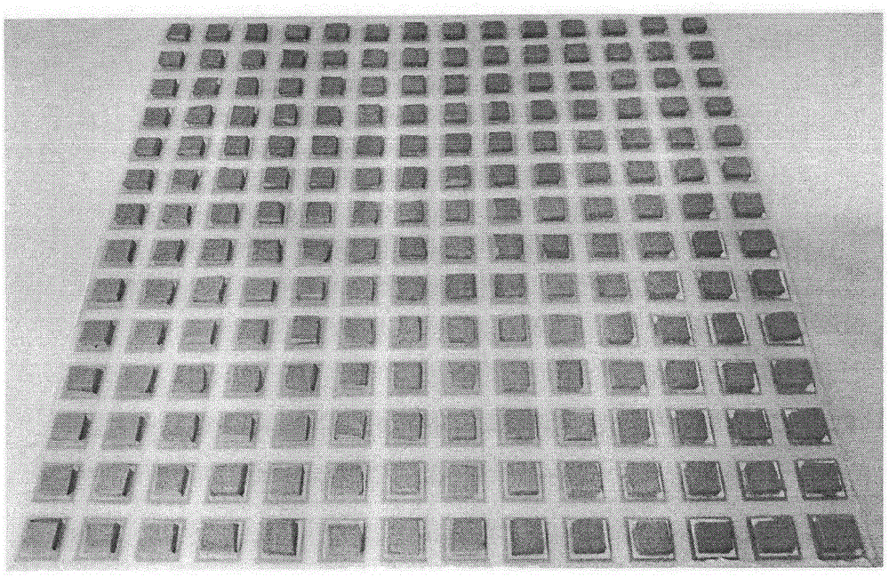
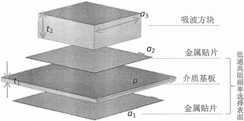
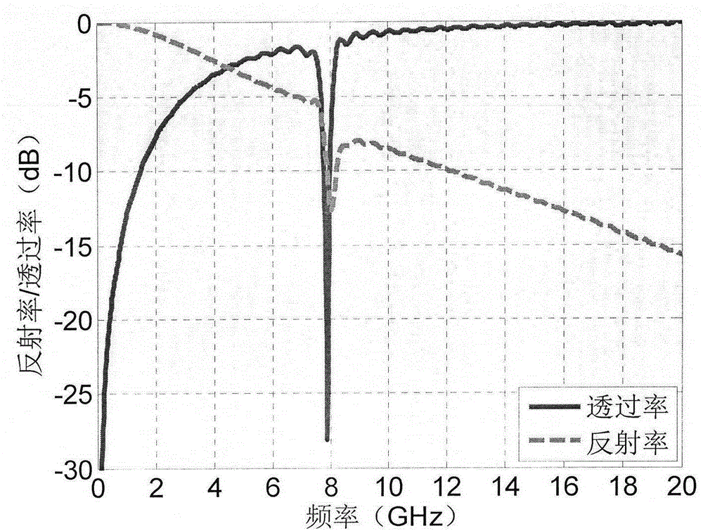
[0028] like Figure 1-2 As shown, the low-pass high-resistance frequency selective surface of this embodiment adopts a double-layer square metal patch structural unit array, and the absorbing unit array adopts an array composed of magnetic absorbing squares. The array of wave-absorbing squares 2 is glued on the low-pass high-resistance frequency selective surface 1, and the geometric centers of the two are coincident. The thickness t=0.017mm of square metal patch 11 and 13, the side lengths of two layers of square metal patch 11 and 13 are respectively: a 1 = 10.4 mm, a 2 =8.7mm. The thickness t of the dielectric substrate 12 1 =0.4mm, relative permittivity ε r =4.3, loss tangent tanδ=0.025. The absorbing square 2 is located on a metal patch with a side length of 8.7 mm, the geometric centers of the two coincide, and the side length of the absorbing square is a 3 =7.0mm, thickness t 2 = 2.4 mm.

[0029] image 3 The electromagnetic wave transmission characteristics of...


PUM


Abstract

The invention discloses a low-pass and high-absorption electromagnetic functional layer, which comprises a low-pass and high-resistance frequency selection surface and a wave absorption unit array, wherein the low-pass and high-resistance frequency selection surface comprises metal structure unit arrays which are etched on two surfaces of a dielectric substrate and are different in structure size; the periods p of the unit arrays are 10.0mm to 20.0mm; metal structure units have rotation symmetry; the frequency selection characteristics of the metal structure units are irrelevant to the polarized direction of an incident wave; the metal structure units on two surfaces are different in size; the wave absorption unit array is a periodic array which comprises square or round sheets which are fabricated by magnetic loss radar wave-absorbing materials or resistance type wave-absorbing materials; the wave absorption unit array has broadband wave absorption performance on a high-frequency band; the sizes of wave absorption units are smaller than those of the metal structure units; and each wave absorption unit is adhered to one side of each metal structure unit with a relatively small size of the low-pass and high-resistance frequency selection surface. The obtained material is small in insertion loss, small in thickness, flexible in design and low in cost.

Description

technical field [0001] The invention relates to the technical field of electromagnetic wave-transmitting materials and wave-absorbing materials, in particular to a low-pass and high-absorption electromagnetic functional layer. Background technique [0002] The electromagnetic functional layer that can efficiently transmit waves within the working frequency band and efficiently absorb waves outside the working frequency band has important application requirements in the fields of anti-jamming communication, electromagnetic protection, and electromagnetic stealth. At present, the design of wave-transmitting materials and wave-absorbing materials is relatively independent, and there is a lack of new electromagnetic materials with high transparency to in-band signals and high absorption of out-of-band signals. Most of the absorbing materials are based on the metal reflective backplane to design their absorbing performance. When the metal backplane is removed, the absorbing perfo...

Claims


Application Information

Patent Timeline
Patent Type & Authority Applications(China)
IPC IPC(8): H01P1/20H01Q17/00H05K9/00
Inventor 王甲富屈绍波马华张介秋庞永强杜红亮
Owner AIR FORCE UNIV PLA
Learn More