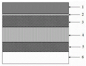
Low-cost solar cell suitable for production
A solar cell, a low-cost technology, applied in circuits, photovoltaic power generation, electrical components, etc., to improve the ability to capture and absorb photons and improve the conversion rate
- Summary
- Abstract
- Description
- Claims
- Application Information
AI Technical Summary
Problems solved by technology
Method used
Image
Examples
Embodiment 1
[0028] 2) Prepare a mixed solution of nickel acetone caproate, lithium acetate, and magnesium acetate tetrahydrate at a molar ratio of 1:1:10, spin-coat it on the light-transmitting / transparent electrode layer, and dry it at 350°C to prepare the electron Transport layer; thickness 99nm;
[0029] 3) Prepare light absorbing layer:
[0030] a. Prepare PbI2 solution, the concentration is 3.0Mol / L, and the solvent is dimethylformamide;
[0031] b. Prepare CH3NH3I solution: concentration 5mg / mL, solvent is isopropanol;
[0032] In-situ synthesis of perovskite materials by solution method: first spin-coat PbI2 solution on the electron transport layer, put it into CH3NH3I solution after drying to soak and grow perovskite materials, and obtain perovskite light-absorbing layer; thickness 53nm;
[0033] 4) Preparation of electron absorbing layer
[0034] The chlorobenzene solution of PCBM is used to spin-coat on the light-absorbing layer, and dry to obtain an electron-absorbing laye...
Embodiment 2
[0042] 2) Prepare a mixed solution of nickel acetone caproate, lithium acetate, and magnesium acetate tetrahydrate at a molar ratio of 2:1:3, spin-coat it on the light-transmitting / transparent electrode layer, and dry it at 360°C to prepare an electronic Transport layer; thickness 85nm;
[0043] 3) Prepare light absorbing layer:
[0044] a. Prepare PbI2 solution, the concentration is 0.5Mol / L, and the solvent is dimethylformamide;
[0045] b. prepare CH3NH3I solution: concentration 10mg / mL, solvent is Virahol;
[0046]In-situ synthesis of perovskite materials by solution method: first spin-coat PbI2 solution on the electron transport layer, put it into CH3NH3I solution after drying to soak and grow perovskite materials, and obtain perovskite light-absorbing layer; thickness 490nm;
[0047] 4) Preparation of electron absorbing layer
[0048] The chlorobenzene solution of PC71BM was used to spin-coat the light-absorbing layer, and dried to obtain an electron-absorbing layer w...
Embodiment 3
[0056] 2) Prepare a mixed solution of nickel acetone caproate, lithium acetate, and magnesium acetate tetrahydrate at a molar ratio of 1:1:5, spin-coat it on the light-transmitting / transparent electrode layer, and dry it at 300°C to prepare the electron Transport layer; the thickness is controlled at 11nm;
[0057] 3) Prepare light absorbing layer:
[0058] a. Prepare PbI2 solution, the concentration is 2.3Mol / L, the solvent is dimethylformamide;
[0059] b. Prepare CH3NH3I solution: concentration 7.5mg / mL, solvent is isopropanol;
[0060] In-situ synthesis of perovskite materials by solution method: first spin-coat PbI2 solution on the electron transport layer, put it into CH3NH3I solution after drying to soak and grow perovskite materials, and obtain perovskite light-absorbing layer; thickness 430nm;
[0061] 4) Preparation of electron absorbing layer
[0062] The chlorobenzene solution of PCBM is used to spin-coat the light-absorbing layer, and dry to obtain an electro...
PUM
 Abstract
Description
Claims
Application Information
 - R&D
- Intellectual Property
- Life Sciences
- Materials
- Tech Scout
- Unparalleled Data Quality
- Higher Quality Content
- 60% Fewer Hallucinations
Browse by: Latest US Patents, China's latest patents, Technical Efficacy Thesaurus, Application Domain, Technology Topic, Popular Technical Reports.
© 2025 PatSnap. All rights reserved.Legal|Privacy policy|Modern Slavery Act Transparency Statement|Sitemap|About US| Contact US: help@patsnap.com

