Photoelectronic material for Zn-doped CuS superlattice nanoflower, preparation method and application thereof
A superlattice and nanoflower technology, applied in the field of nanomaterials, can solve the problems of difficult industrial production, complex process equipment, strict operation requirements, etc., and achieve the effects of simple operation, simple process and wide application prospects.
- Summary
- Abstract
- Description
- Claims
- Application Information
AI Technical Summary
Problems solved by technology
Method used
Image
Examples
Embodiment 1
[0044]Add 0.5mmol CuCl, 0.75mmol S powder and 15mL absolute ethanol to a polytetrafluoroethylene liner of a 20mL reaction kettle, and then seal the reaction kettle after magnetic stirring for 10 minutes, place it in a constant temperature drying oven, control the temperature at 180°C, and react at a constant temperature 24 hours, naturally cooled to room temperature. The obtained product was washed twice with distilled water and absolute ethanol successively, separated by centrifugation, and dried at 60° C. for 30 minutes in a vacuum oven (0.1 Pa) to obtain a black solid powder product.
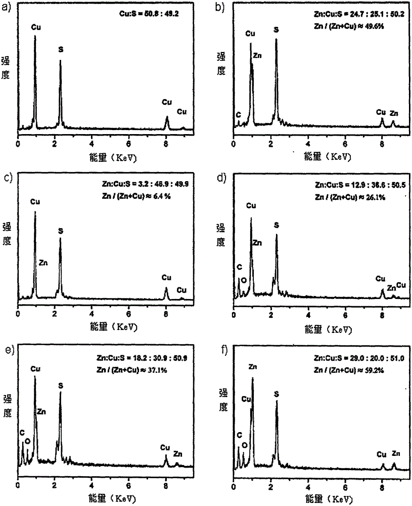
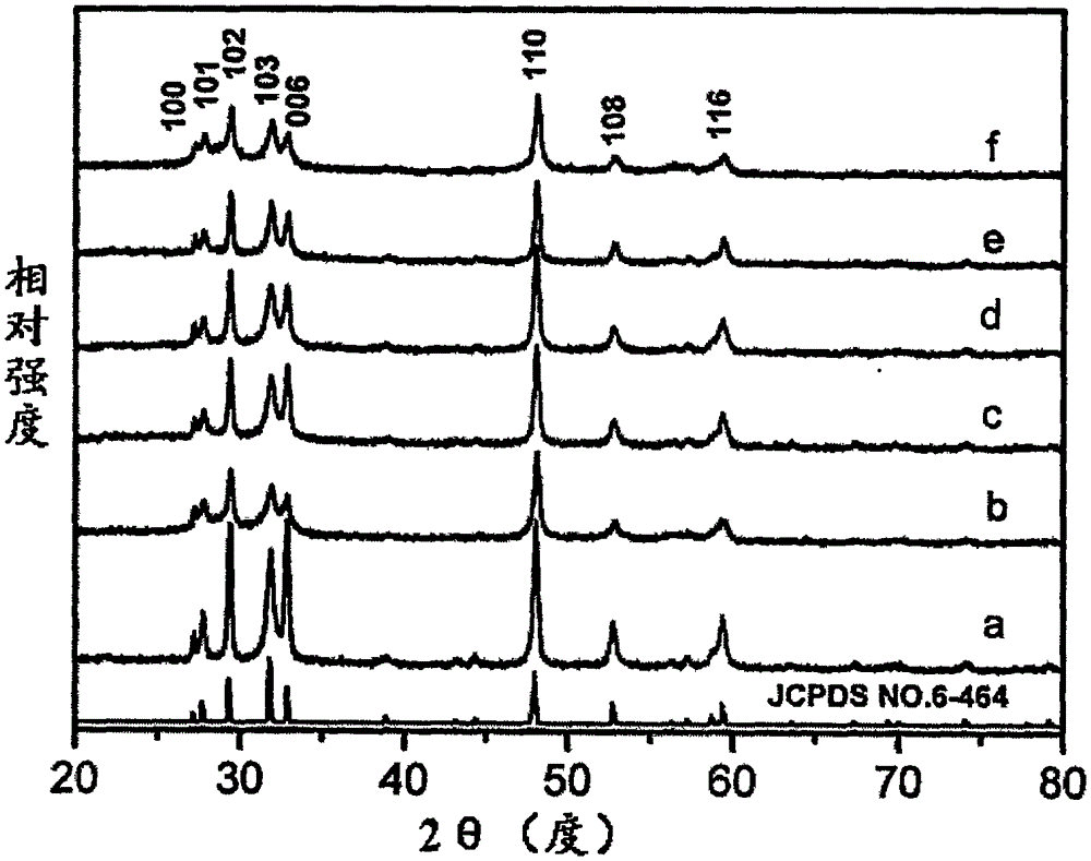
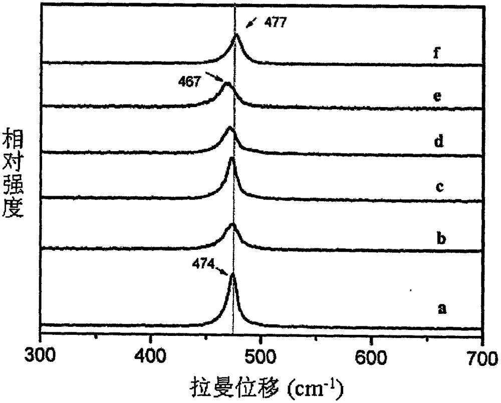
[0045] Product analysis results: the chemical composition of the product is pure CuS (Cu:S=50.2:49.8) through EDS elemental analysis. Powder X-ray diffraction (XRD) analysis shows that the pure CuS product is a hexagonal crystal phase, and the unit cell parameters Raman spectrum active mode vibration frequency peak appears at 474cm -1 , which is consistent with the vibration frequency of...
Embodiment 2
[0047] Add 0.25mmol CuCl, 0.25mmol Zn(Ac) 2 2H 2 O, 0.75mmol S powder and 15mL absolute ethanol were stirred magnetically for 10 minutes, sealed the reaction vessel, placed in a constant temperature drying oven, controlled at a temperature of 180°C, reacted at a constant temperature for 24 hours, and cooled naturally to room temperature. The obtained product was washed twice with distilled water and absolute ethanol successively, separated by centrifugation, and dried at 60° C. for 30 minutes in a vacuum oven (0.1 Pa) to obtain a black solid powder product.
[0048] Product analysis results: The chemical composition of the product is Zn by EDS elemental analysis 0.49 Cu 0.51 S (Zn:Cu:S=24.7:25.1:50.2, Zn / (Zn+Cu)=49.6%). The scanning electron microscope (SEM) photo observation product has a flower-like micromorphology, the particle size of the flower is about 1 μm, and the petal thickness is about 30 nm. Powder X-ray diffraction (XRD) analysis shows that all X-ray diffracti...
Embodiment 3
[0050] Add 0.45mmol CuCl, 0.05mmol Zn(Ac) 2 2H 2 O, 0.75mmol S powder and 15mL absolute ethanol were stirred magnetically for 10 minutes, sealed the reaction vessel, placed in a constant temperature drying oven, controlled at a temperature of 180°C, reacted at a constant temperature for 24 hours, and cooled naturally to room temperature. The obtained product was washed twice with distilled water and absolute ethanol successively, separated by centrifugation, and dried at 60° C. for 30 minutes in a vacuum oven (0.1 Pa) to obtain a black solid powder product.
[0051] Product analysis results: The chemical composition of the product is Zn by EDS elemental analysis 0.06 Cu 0.94 S (Zn:Cu:S=3.2:46.9:49.9, Zn / (Zn+Cu)=6.4%). The scanning electron microscope (SEM) photo observation product has a flower-like micromorphology, the particle size of the flower is about 1 μm, and the petal thickness is about 30 nm. Powder X-ray diffraction (XRD) analysis shows that all X-ray diffraction...
PUM
| Property | Measurement | Unit |
|---|---|---|
| Particle size | aaaaa | aaaaa |
| Thickness | aaaaa | aaaaa |
Abstract
Description
Claims
Application Information
 - R&D
- Intellectual Property
- Life Sciences
- Materials
- Tech Scout
- Unparalleled Data Quality
- Higher Quality Content
- 60% Fewer Hallucinations
Browse by: Latest US Patents, China's latest patents, Technical Efficacy Thesaurus, Application Domain, Technology Topic, Popular Technical Reports.
© 2025 PatSnap. All rights reserved.Legal|Privacy policy|Modern Slavery Act Transparency Statement|Sitemap|About US| Contact US: help@patsnap.com


