
Laser and grating coupler packaging structure and method

A technology of grating coupler and packaging structure, which is applied in the coupling of semiconductor laser optical devices, lasers, and optical waveguides, etc., to avoid unstable performance, reduce coupling loss, and simple structure.

Active Publication Date: 2016-01-20
WUHAN TELECOMM DEVICES
View PDF9 Cites 31 Cited by
  • Summary
  • Abstract
  • Description
  • Claims
  • Application Information

AI Technical Summary

Problems solved by technology

However, there has not been a design that fully meets the performance requirements. Therefore, in silicon-based monolithic integrated optoelectronic chips, the relatively simple and feasible way is to use external hybrid integration of Group III and V lasers to realize the function of the light source.

Method used


Image

  • Laser and grating coupler packaging structure and method
  • Laser and grating coupler packaging structure and method
  • Laser and grating coupler packaging structure and method

Examples


Embodiment Construction

[0028] The present invention will be described in further detail below in conjunction with specific embodiments and accompanying drawings. Examples of the described embodiments are shown in the drawings, wherein like or similar reference numerals designate like or similar elements or elements having the same or similar functions throughout. The embodiments described below with reference to the accompanying drawings are exemplary, and are only used to explain the technical solution of the present invention, and should not be construed as limiting the present invention.

[0029] In the description of the present invention, the terms "inner", "outer", "longitudinal", "transverse", "upper", "lower", "top", "bottom" or "front", "rear", "left ", "right" and other indicated orientations or positional relationships are based on the orientations or positional relationships shown in the drawings, and are only for the convenience of describing the present invention and do not require tha...


PUM


Abstract

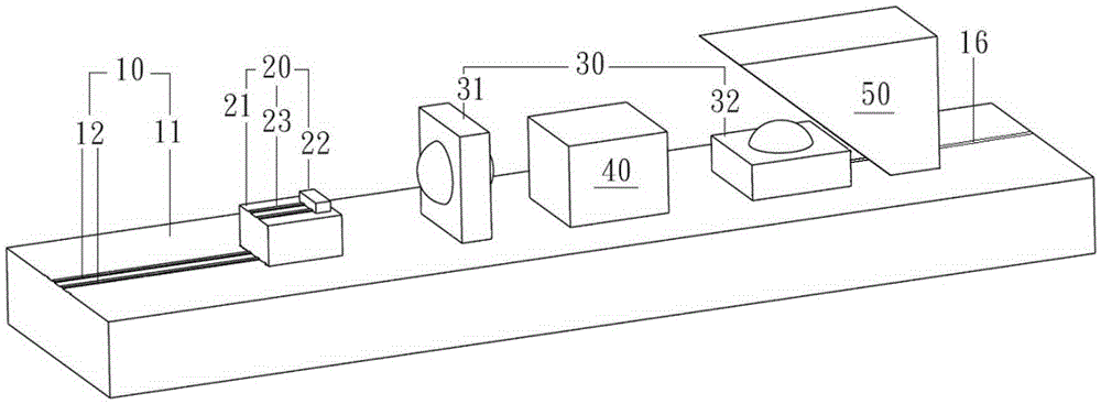
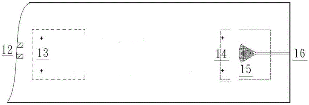
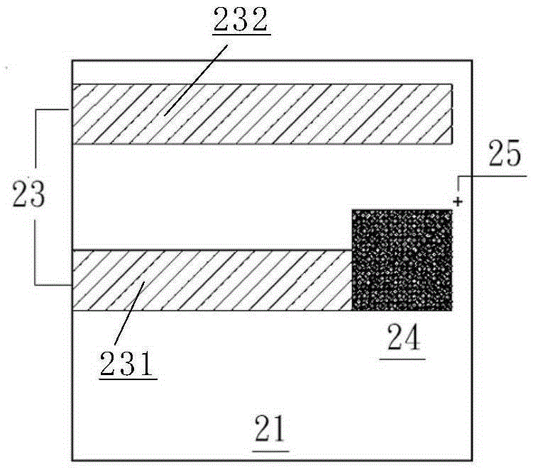
The invention provides a laser and grating coupler packaging structure and method. The packaging structure comprises a laser unit, a collimating lens, an isolator and a reflection prism, wherein the laser unit, the collimating lens, the isolator and the reflection prism are mounted on a silicon-based photoelectric chip. The silicon-based photoelectric chip comprises a first electrode, first and second marks, a grating coupler and a waveguide layer which are all arranged at the surface; the laser unit comprises a transitional substrate and a laser; the collimating lens comprises a first lens and a second lens, the first lens is vertical to the surface, the second lens is arranged at the surface at the position of the second mark, and thus, the grating coupler is placed in the central area of the main axis of the optical path of the second lens; and the isolator is mounted at the surface between the first lens and the second lens, so that diverging light output by the laser is collimated by the first lens, then reflected to the reflection prism through the isolator, deflected by the reflection prism for certain angle, and gathered by the second lens, and the gathering point is placed at the surface of the grating coupler. Thus, technical problems in accurate in-place packaging are solved, convenience is provided for preparation, and the yield rate is improved.

Description

technical field [0001] The invention provides a silicon photonic integrated device, in particular to provide a packaging structure of a laser and a grating coupler and a method thereof. Background technique [0002] Silicon-based monolithic integrated optoelectronic chips are currently a hot spot in international research. Silicon-based optoelectronic integration technology is to monolithically integrate optical waveguides / modulators, photodetectors, drive circuits and receiver circuits, that is, optical components It is integrated with electrical components on a chip, and all devices are manufactured using standard integrated circuit technology. Its advantages are mature manufacturing technology, low cost, and small size, and is suitable for short- and medium-distance optical communication applications such as data centers. [0003] Although silicon-based materials can be used to make most of the optical devices and electrical devices in optical fiber communication, since s...

Claims


Application Information

Patent Timeline
Patent Type & Authority Applications(China)
IPC IPC(8): G02B6/42H01S5/0238
CPCG02B6/4204G02B6/4214G02B6/4219G02B6/4296H01S5/0238H01S5/005H01S5/0064H01S5/0071G02B6/4206G02B6/4209H01S5/0225H01S5/02345H01S5/02325H01S5/02253G02B6/34H01S3/0071H01S5/0261
Inventor 李世瑜张玓胡胜磊余少华
Owner WUHAN TELECOMM DEVICES
Learn More