


Quick Research
Generate reliable direction feasibility study reports for your R&D in just a few steps.

Technical Q&A
Discover and master advanced knowledge NOW. Basics, ideas, possibilities, all at once.

Find Solutions
As an expert in R&D theories, this can generate solutions to your technical problems instantly.

Evaluate Feasibility
Analyze your overall solution with one click, know your potential R&D risks in advance.

Monitor Landscape
Get weekly tech updates, stay abreast of the latest tech innovations and key insights.
LED epitaxial growth method
An epitaxial growth, N-type technology, used in electrical components, circuits, semiconductor devices, etc., can solve the problems of low hole transport and injection efficiency, low Mg activation efficiency, low hole mobility, etc. Improve activation efficiency and light effect
- Summary
- Abstract
- Description
- Claims
- Application Information
AI Technical Summary
Problems solved by technology
Method used
Image


Examples
Embodiment 1
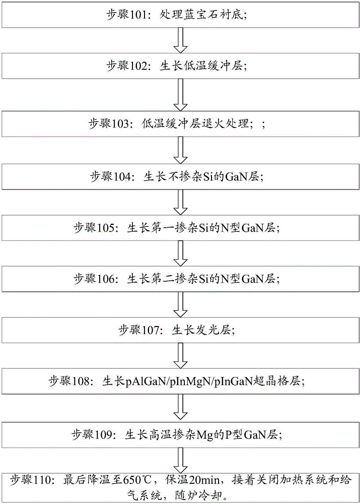
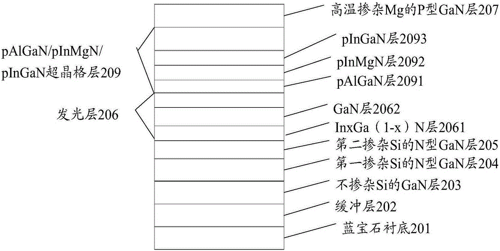
[0048] combine figure 1 with figure 2 , this embodiment provides a LED epitaxial growth method, specifically as follows:
[0049] Step 101, processing the sapphire substrate 201: in a hydrogen atmosphere at 1000°C, inject 100 L / min of H2, keep the reaction chamber pressure at 100 mbar, and process the sapphire substrate 201 for 8 minutes;
[0050] Step 102, grow low-temperature buffer layer 202: lower the temperature to 500°C, keep the reaction chamber pressure at 300mbar, feed NH3 at a flow rate of 10000sccm, TMGa at 50sccm, and H2 at 100L / min, and grow a 20nm-thick sapphire substrate 201 Low temperature buffer layer 202;
[0051] Step 103, annealing the low-temperature buffer layer 202: raise the temperature to 1000°C, keep the pressure in the reaction chamber at 300mbar, feed in NH3 at a flow rate of 30000sccm, H2 at 100L / min, and keep the temperature stable at 300°C to corrode the low-temperature buffer layer 202 into irregular islands;
[0052] Step 104, grow the N-t...
Embodiment 2
[0064] This embodiment provides an LED epitaxial growth method, specifically as follows:
[0065] Step 201, processing the sapphire substrate 201: in a hydrogen atmosphere at 1100°C, inject 130 L / min of H2, keep the reaction chamber pressure at 300 mbar, and process the sapphire substrate 201 for 10 minutes;
[0066] Step 202, grow low-temperature buffer layer 202: lower the temperature to 600°C, keep the reaction chamber pressure at 600mbar, feed NH3 at a flow rate of 20,000sccm, TMGa at 100sccm, and H2 at 130L / min, and grow a sapphire substrate 201 with a thickness of 40nm Low temperature buffer layer 202;
[0067] Step 203, annealing the low-temperature buffer layer 202: raise the temperature to 1100°C, keep the reaction chamber pressure at 600mbar, feed in NH3 at a flow rate of 40,000sccm, and H2 at 130L / min, and keep the temperature stable at 500°C to corrode the low-temperature buffer layer 202 into irregular islands;
[0068] Step 204, grow the N-type GaN layer 203 no...
Embodiment 3
[0080] Step 301, processing the sapphire substrate 201: in a hydrogen atmosphere at 1050°C, inject 115 L / min of H2, keep the reaction chamber pressure at 200 mbar, and process the sapphire substrate 201 for 9 minutes;
[0081] Step 302, grow the low-temperature buffer layer 202: lower the temperature to 550°C, keep the reaction chamber pressure at 450mbar, feed NH3 at a flow rate of 15000sccm, TMGa at 75sccm, and H2 at 115L / min, and grow a 30nm-thick sapphire substrate 201 Low temperature buffer layer 202;
[0082] Step 303, annealing the low-temperature buffer layer 202: raise the temperature to 1050°C, keep the pressure of the reaction chamber at 450mbar, feed in NH3 at a flow rate of 35000sccm, and H2 at 115L / min, and keep the temperature stable at 400°C to corrode the low-temperature buffer layer 202 into irregular islands;
[0083] Step 304, grow the N-type GaN layer 203 not doped with Si: raise the temperature to 1100°C, keep the reaction chamber pressure at 450mbar, fe...
PUM
 Abstract
Description
Claims
Application Information
 - R&D Engineer
- R&D Manager
- IP Professional
- Industry Leading Data Capabilities
- Powerful AI technology
- Patent DNA Extraction
Browse by: Latest US Patents, China's latest patents, Technical Efficacy Thesaurus, Application Domain, Technology Topic, Popular Technical Reports.
© 2024 PatSnap. All rights reserved.Legal|Privacy policy|Modern Slavery Act Transparency Statement|Sitemap|About US| Contact US: help@patsnap.com