
Method for preparing ceramic substrate containing conductive copper cylinder

A technology of ceramic substrates and ceramic substrates, which is applied in semiconductor/solid-state device manufacturing, circuits, electrical components, etc., can solve problems such as difficult interconnection, usage restrictions, and serious pollution of three wastes, so as to improve yield and reliability, The effect of excellent performance and simple process

Active Publication Date: 2015-12-30
武汉利之达科技股份有限公司
View PDF4 Cites 10 Cited by
  • Summary
  • Abstract
  • Description
  • Claims
  • Application Information

AI Technical Summary

Problems solved by technology

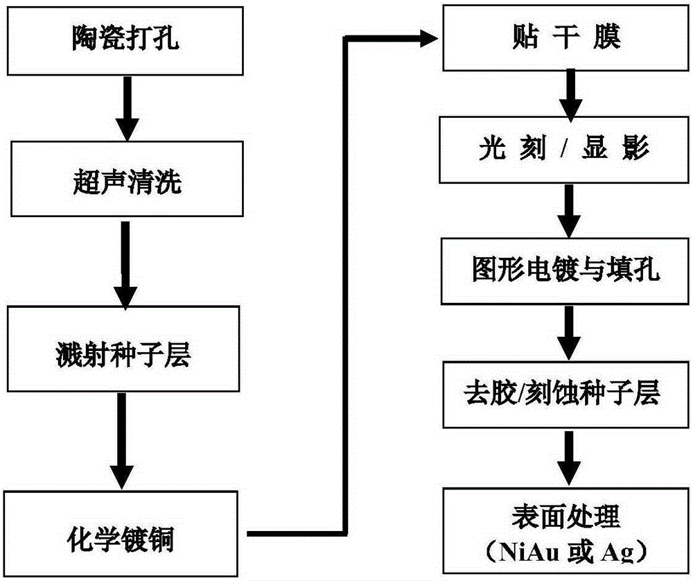
However, for straight holes with small diameter and relatively large depth diameter, the full coverage of the metal layer on the hole wall cannot be achieved, making the electroplated copper structure in the hole discontinuous and difficult to achieve interconnection; 2) The metallization of the hole wall is achieved by using electroless plating technology like figure 1 shown
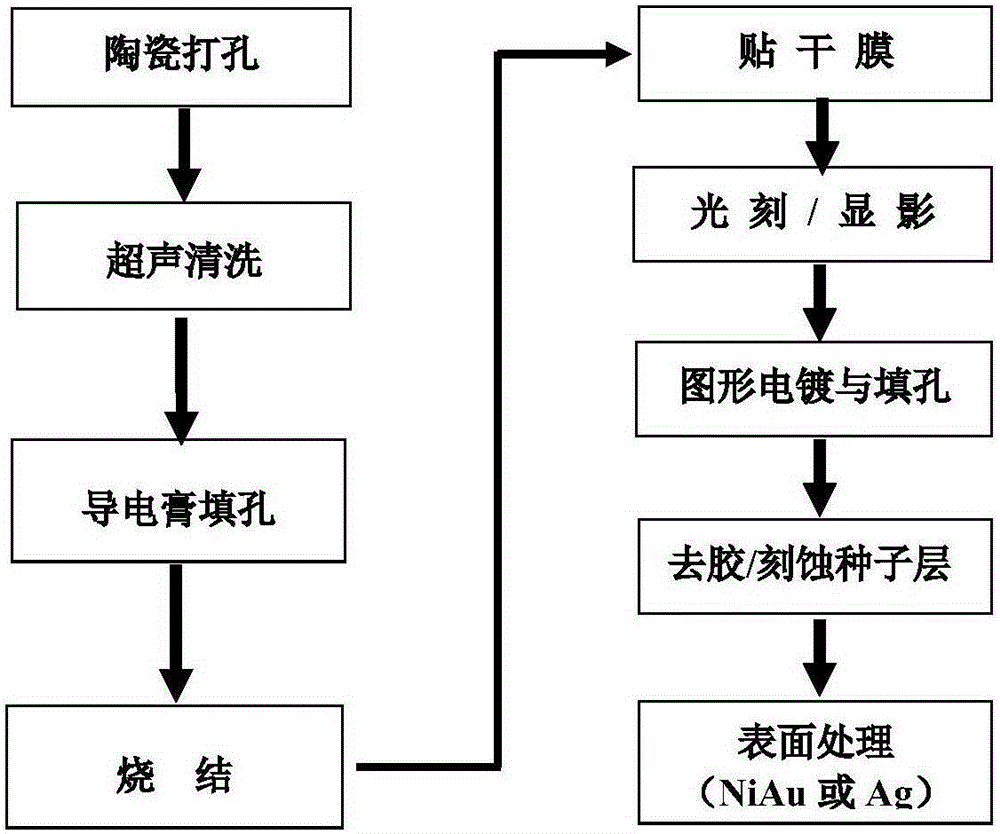
The disadvantage is that the electroless plating process is complicated, the pollution of the three wastes is serious (the reducing agent formaldehyde is harmful), and the use is greatly restricted; 3) The through hole is directly filled with a conductive polymer (such as a conductive paste or conductive adhesive), such as figure 2
The disadvantage is that it is difficult to fill the small holes. After filling the holes, it needs to be heated and cured (sintered), and the electrical and thermal conductivity of the filler is poor.

Method used


Image

  • Method for preparing ceramic substrate containing conductive copper cylinder
  • Method for preparing ceramic substrate containing conductive copper cylinder
  • Method for preparing ceramic substrate containing conductive copper cylinder

Examples


Embodiment 1

[0023] The processing steps of this embodiment are:

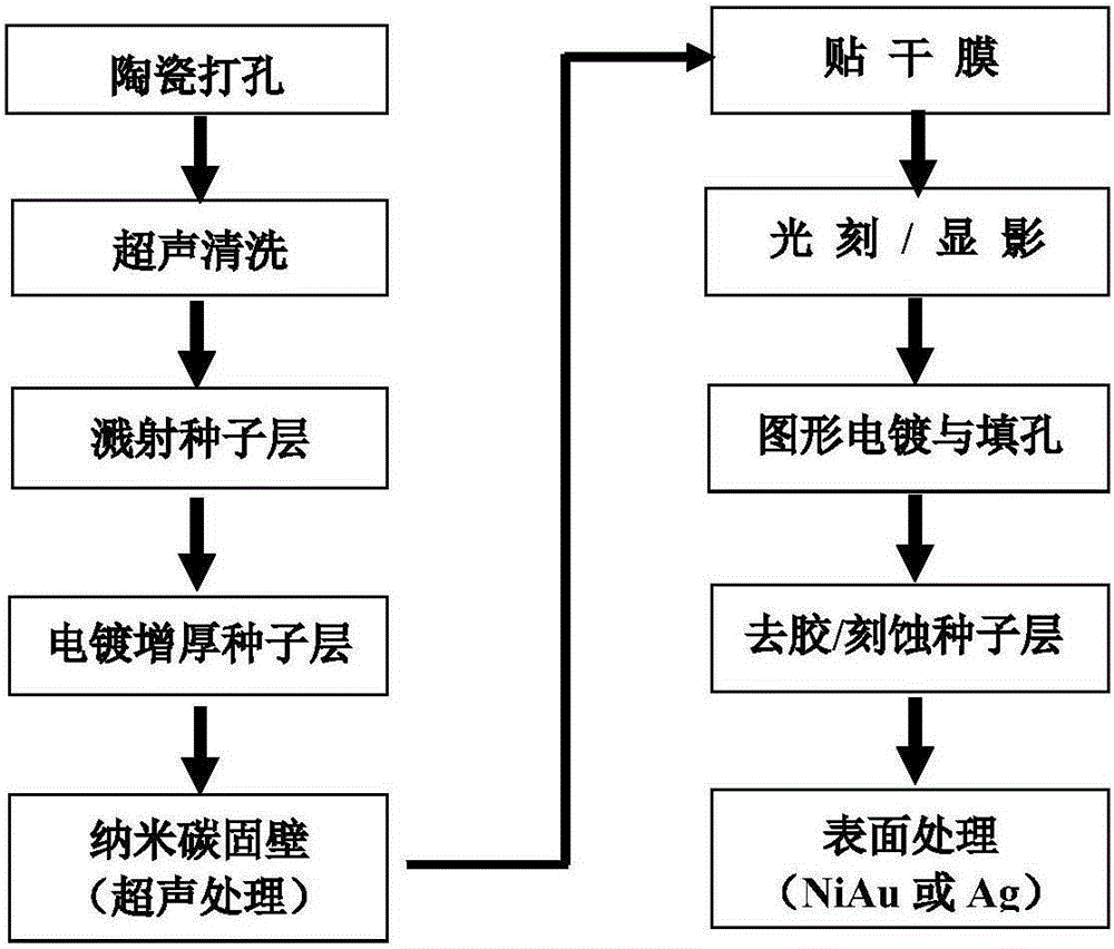
[0024] 1) Drilling: using a laser to prepare an array of through-holes with a diameter of 100um on the alumina ceramic substrate (thickness: 0.5mm);

[0025] 2) Pretreatment: ultrasonically clean the ceramic substrate in deionized water, acetone, and ethanol solution for 5 minutes, and then dry it (100°C, 30 minutes);

[0026] 3) Sputtering coating: the ceramic substrate is placed in a coating machine, and 200nm titanium (Ti) and 200nm copper (Cu) are sequentially deposited on the surface of the substrate by a sputtering process as a seed layer;

[0027] 4) Thickening of electroplating: the whole board electroplating copper technology is adopted to increase the thickness of the seed layer to 3 μm;

[0028] 5) Prepare wall-solidifying solution: Stir and mix 1 gram of graphene, 100 grams of deionized water, and 1 ml of sodium hexametaphosphate, and adjust the pH value of the solution to 10.0 with potassium hydroxide;

[002...

Embodiment 2

[0035] The processing steps of this embodiment are:

[0036] 1) Drilling: using a laser to prepare an array of through holes with a diameter of 200um on the aluminum nitride ceramic substrate (thickness: 1.0mm);

[0037] 2) Pretreatment: ultrasonically clean the ceramic substrate in deionized water, acetone, and ethanol solution for 5 minutes, and then dry it (100°C, 30 minutes);

[0038] 3) Sputtering coating: the ceramic substrate is placed in a coating machine, and 100nm titanium (Ti) and 200nm copper (Cu) are sequentially deposited on the surface of the substrate by a sputtering process as a seed layer;

[0039] 4) Thickening of electroplating: the whole board electroplating copper technology is adopted to increase the thickness of the seed layer to 5 μm;

[0040] 5) Prepare wall-solidifying solution: Stir and mix 3 grams of nano-graphite flakes, 100 grams of deionized water, and 2 ml of sodium alkylphosphocarboxylate, and adjust the pH value of the solution to 10.5 with ...

Embodiment 3

[0047] The processing steps of this embodiment are:

[0048] 1) Drilling: using a laser to prepare an array of through holes with a diameter of 50um on the beryllium oxide ceramic substrate (thickness: 0.38mm);

[0049] 2) Pretreatment: ultrasonically clean the ceramic substrate in deionized water, acetone, and ethanol solution for 5 minutes, and then dry it (100°C, 30 minutes);

[0050] 3) Sputtering coating: the ceramic substrate is placed in a coating machine, and 100nm titanium (Ti) and 200nm copper (Cu) are sequentially deposited on the surface of the substrate by a sputtering process as a seed layer;

[0051] 4) Thickening of electroplating: the whole board electroplating copper technology is adopted to increase the thickness of the seed layer to 2 μm;

[0052] 5) Prepare wall-solidifying solution: Stir and mix 5 grams of nano-carbon powder, 100 grams of deionized water, and 3 ml of sodium dodecylbenzenesulfonate, and adjust the pH value of the solution to 9.5 with pota...


PUM


Abstract

The invention provides a method for preparing a ceramic substrate containing a conductive copper cylinder. The method includes the steps that first, through holes are prepared in the ceramic substrate through a laser boring technology; then a metal seed layer is deposited on the surface of the substrate through a sputtering technology, and the thickness of the seed layer is increased through electroplating; afterwards, the substrate is soaked in a wall bracing solution made of a carbon nanomaterial, and a conducting film is formed on each hole wall under the action of ultrasound or jet; at last, the ceramic substrate with the surface being provided with a metal circuit and internally provided with the conductive copper cylinder is prepared through the pattern electroplating and corrosion technology. Due to the facts that the carbon nanomaterial is good in electricity-conducting and heat-conducting property and the binding force of the carbon nanomaterial and ceramic is high, the performance and reliability of the ceramic substrate are improved. Meanwhile, the nanocarbon wall bracing technology is adopted for preparing the conductive copper cylinder. Compared with an existing chemical plating and conducting polymer hole-filling technology, the method has the advantages of being simple in technology, environmentally friendly in material, low in cost, suitable for mass production and the like.

Description

technical field [0001] The invention belongs to the field of electronic manufacturing, in particular to a method for preparing a ceramic substrate containing conductive copper pillars. Background technique [0002] With the development of three-dimensional packaging technology and the improvement of system integration, in the manufacturing process of power devices represented by high-power light-emitting diodes (LEDs), insulated gate bipolar transistors (IGBTs), and laser diodes (LDs), the preparation and Selection becomes a key technical link, and directly affects the performance and reliability of the device. Taking high-power LED devices as an example, since 70%-80% of the input electric power is converted into heat (only about 20%-30% is converted into light energy), and the LED chip area is small, the power density of the device is large (greater than 100W / cm 2 ), so heat dissipation has become a key technology that must be solved for high-power LED packaging. If the ...

Claims


Application Information

Patent Timeline
IPC IPC(8): C04B41/85C04B41/90H01L21/48
Inventor 陈明祥刘松坡程浩陈珍
Owner 武汉利之达科技股份有限公司
Learn More