Solution-processed organic-inorganic planar heterojunction light emitting diode and manufacturing method thereof
A technology of light-emitting diodes and solution processing, which is applied to the materials of organic semiconductor devices, semiconductor/solid-state device manufacturing, nanotechnology for materials and surface science, etc., which can solve the imbalance of electron and hole transport and the difficulty of achieving monochromatic Solve the problems of light source and luminescence peak shape, etc., achieve the effect of sharp luminescence peak, overcome high material cost, and narrow half-peak width
- Summary
- Abstract
- Description
- Claims
- Application Information
AI Technical Summary
Problems solved by technology
Method used
Image
Examples
Embodiment 1
[0044] Preparation of light-emitting layer materials:
[0045] Dissolve compound A, compound B and polymer additives in an organic solvent and stir until the reaction is complete; the compound A is an organic or inorganic salt containing a halogen; the compound B is a metal inorganic salt containing a halogen; the compound A The molar ratio to compound B is 1:1-10:1; the added amount of the polymer additive is 0.5%-15% of the mass sum of compound A and compound B.
[0046] Compound A (CH 3 NH 3 I,CH 3 NH 3 Br,CH 3 NH 3 Cl,CH 3 CH 2 NH 3 I,CH 3 CH 2 NH 3 Br,CH 3 CH 2 NH 3 Cl,CH 3 CH 2 CH 2 NH 3 I,CH 3 CH 2 CH 2 NH 3 Br,CH 3 CH 2 CH 2 NH 3 Cl, CsI, CsBr, CsCl, CH(NH 2 ) 2 I,CH(NH 2 ) 2 Br,CH(NH 2 ) 2 Cl,CH 3 CH(NH 2 ) 2 I,CH 3 CH(NH 2 ) 2 Br,CH 3 CH(NH 2 ) 2 Cl) was synthesized according to the method in the literature (J.Am.Chem.Soc.2012,134,17396-17399).
[0047] Compound B is at least one of the following compounds: PbI 2 ,PbBr 2 ,P...
Embodiment 2
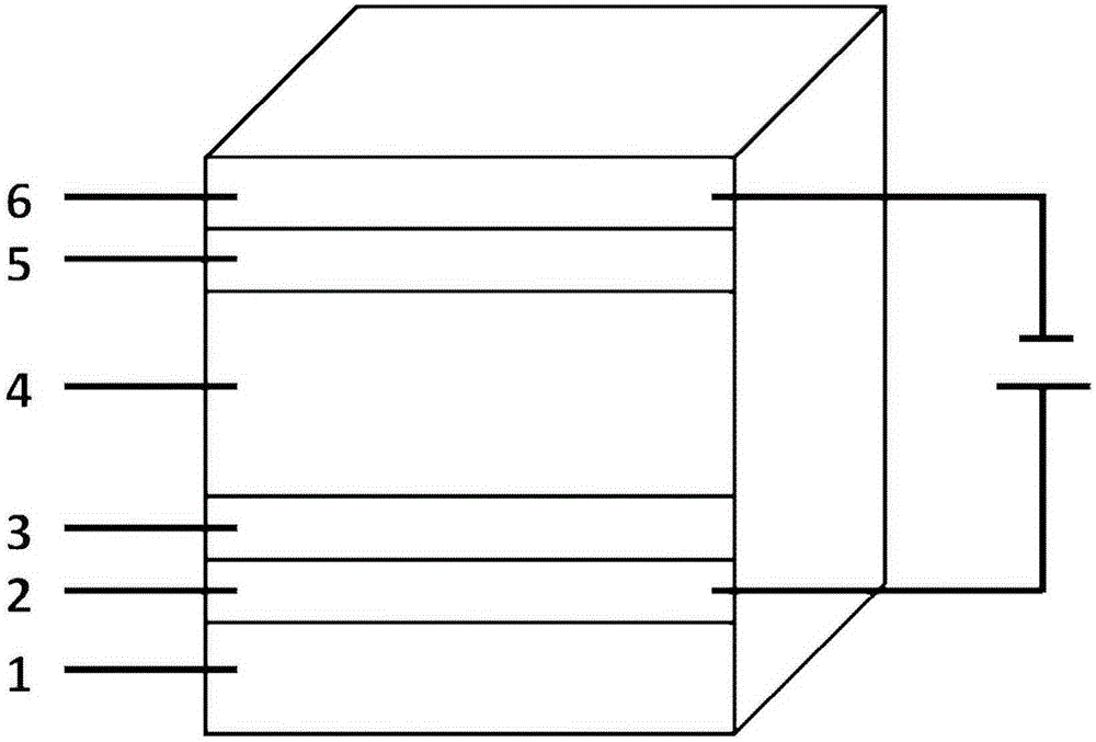
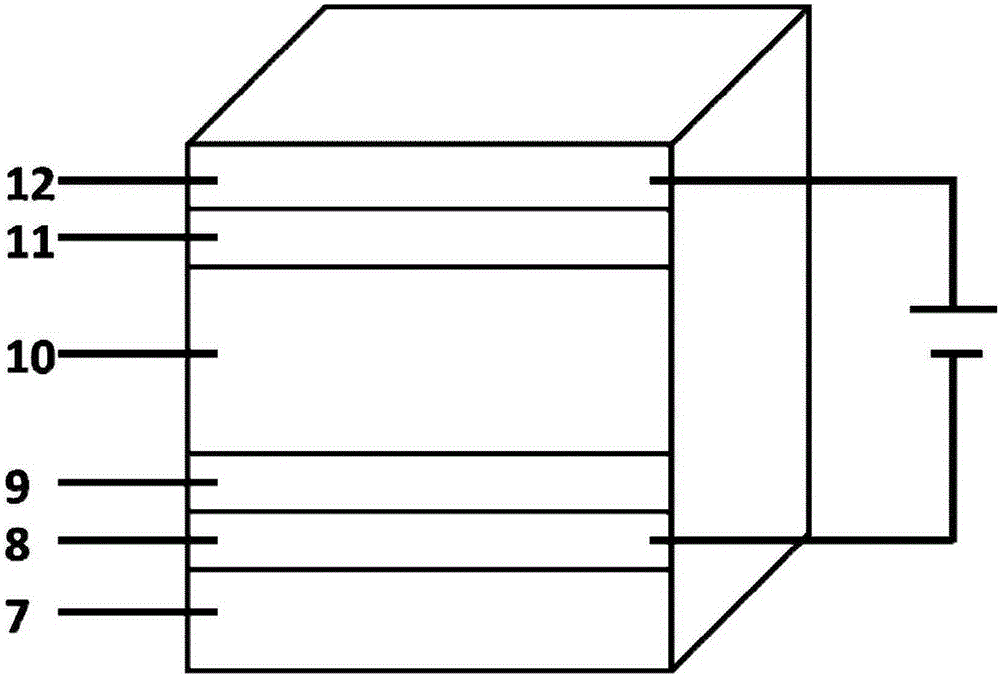
[0057] Fabrication of organic-inorganic heterojunction light-emitting diodes:
[0058]Pre-cut the ITO conductive glass with a square resistance of 20 ohms / cm2 into 15mm×15mm square pieces. Use acetone, special detergent for micron-sized semiconductors, deionized water, and isopropanol to clean ultrasonically in sequence, blow dry with nitrogen, and place in a constant temperature oven for later use. Before use, the ITO glass slides were bombarded with plasma in an oxygen plasma etcher for 4 minutes. PEDOT:PSS aqueous dispersion (about 1%) was purchased from Bayer Company, and the buffer layer was spin-coated at a high speed with a homogenizer (KW-4A), and the thickness was determined by the solution concentration and rotating speed. 500 type) measured monitoring. After the film is formed, the residual solvent is removed in a constant temperature vacuum oven. The film thickness of PEDOT:PSS on the ITO substrate is preferably about 40 nanometers. The cathode interface layer ...
Embodiment 3
[0073] Luminescence properties of organic-inorganic heterojunction light-emitting diodes with different light-emitting layer materials.
[0074] CH 3 NH 3 PB 3 , CH 3 NH 3 PbBr 3 and CH 3 NH 3 PbBr x Cl 3-x The luminescent performance of the organic-inorganic heterojunction light-emitting diode prepared for the light-emitting layer material was measured, and the results are shown in Table 2. to CH 3 NH 3 PB 3 and CH 3 NH 3 PbBr 3 The electroluminescence spectrum is scanned, and the results are as follows Figure 8 .
[0075] Table 2 Light-emitting diode device performance indicators of different light-emitting layer materials
[0076]
[0077] It can be seen from Table 2 that by changing the material of the light-emitting layer, the performance of the light-emitting diode will be changed to a certain extent. And different light-emitting layer materials will emit different light colors, CH 3 NH 3 PB 3 emits red light, while CH 3 NH 3 PbBr 3 and CH 3 ...
PUM
| Property | Measurement | Unit |
|---|---|---|
| external quantum efficiency | aaaaa | aaaaa |
Abstract
Description
Claims
Application Information
 - R&D
- Intellectual Property
- Life Sciences
- Materials
- Tech Scout
- Unparalleled Data Quality
- Higher Quality Content
- 60% Fewer Hallucinations
Browse by: Latest US Patents, China's latest patents, Technical Efficacy Thesaurus, Application Domain, Technology Topic, Popular Technical Reports.
© 2025 PatSnap. All rights reserved.Legal|Privacy policy|Modern Slavery Act Transparency Statement|Sitemap|About US| Contact US: help@patsnap.com


