
Quantum dot display device and manufacturing method thereof

A technology of a display device and a manufacturing method, which is applied to electronic equipment, other household appliances, applications, etc., can solve the problems of cumbersome process, difficulty in obtaining a large-size, high-resolution display device, waste of materials, etc.

Active Publication Date: 2015-12-02
TCL CHINA STAR OPTOELECTRONICS TECH CO LTD
View PDF6 Cites 39 Cited by
  • Summary
  • Abstract
  • Description
  • Claims
  • Application Information

AI Technical Summary

Problems solved by technology

[0005] When making quantum dot patterns in existing quantum dot display devices, the quantum dot materials are usually first mixed with red, green, and blue color photoresist correspondingly, then exposed and developed to form a pattern containing quantum dots, and then continue to make The lower polarizing layer and the alignment layer are used to obtain a color filter substrate, and finally the color filter substrate and the array substrate are paired into a box to make a quantum dot display device. However, this method needs to separate the red, green, and blue quantum dots in advance Mixing with red, green, and blue color photoresist, the process is cumbersome, and it is also very difficult to disperse quantum dots evenly in the color photoresist
In addition to the above methods, quantum dot patterns can also be produced by transfer printing, screen printing and other methods, but these methods have serious waste of materials, poor process repeatability, and the prepared quantum dot patterns are poor in fineness, and it is difficult to obtain large size, high-resolution display

Method used


Image

  • Quantum dot display device and manufacturing method thereof
  • Quantum dot display device and manufacturing method thereof
  • Quantum dot display device and manufacturing method thereof

Examples


Embodiment Construction

[0048] In order to further illustrate the technical means adopted by the present invention and its effects, the following describes in detail in conjunction with preferred embodiments of the present invention and accompanying drawings.

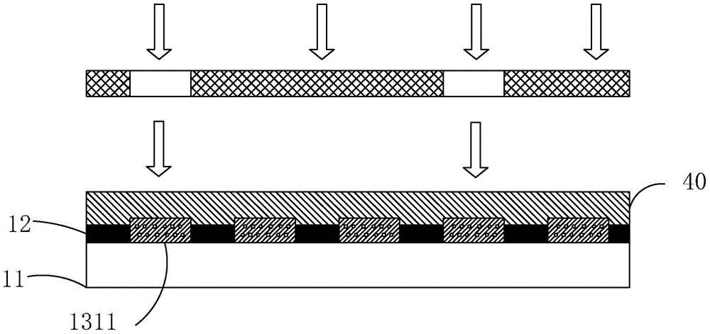
[0049] see Figure 9 The present invention firstly provides a quantum dot display device, comprising: a color filter substrate 1, an array substrate 2 disposed opposite to the color filter substrate 1, a blue light backlight module 4 disposed below the color filter substrate 1, and A liquid crystal layer 3 interposed between the color filter substrate 1 and the array substrate 2;

[0050] The color filter substrate 1 includes: a lower substrate 11, a color filter layer 13 and a black matrix 12 arranged on the lower substrate 11, a lower polarizing layer 14 arranged on the color filter layer 13, and a lower polarizing layer 14 arranged on the lower substrate 11. The lower alignment layer 15 on the lower polarizing layer 14;

[0051] The color...


PUM


Abstract

The invention provides a quantum dot display device and a manufacturing method thereof. According to the quantum dot display device, a colorful filter layer has exquisite quantum dot patterns, and therefore the display device has the higher resolution, color saturation and color gamut, and is reasonable in structure, so that the manufacturing technology of the quantum dot display device is simple. According to the manufacturing method of the quantum dot display device, by means of existing coating, exposure, development and other processes of an existing color filter, the exquisite quantum dot patterns are obtained by manufacturing red and green quantum dot resin compositions containing surface modification, and then the quantum dot display device with the high resolution, color saturation and color gamut is obtained. According to the method, the raw material preparation and manufacturing technology is simple, few materials are consumed, the production cost is low, and the quantum dot display device is applicable to mass production.

Description

technical field [0001] The invention relates to the field of display technology, in particular to a quantum dot display device and a manufacturing method thereof. Background technique [0002] A liquid crystal display (Liquid Crystal Display, LCD) has many advantages such as a thin body, power saving, and no radiation, and has been widely used. Such as: LCD TV, mobile phone, personal digital assistant (PDA), digital camera, computer screen or notebook computer screen, etc., occupy a dominant position in the field of flat panel display. [0003] The working principle of the liquid crystal display is to pour liquid crystal molecules between the thin film transistor array substrate (ThinFilmTransistorArraySubstrate, TFTArraySubstrate) and the color filter substrate (ColorFilterSubstrate, CFSubstrate), and apply a driving voltage on the two substrates to control the rotation direction of the liquid crystal molecules , to refract the light from the backlight module to generate a...

Claims


Application Information

Patent Timeline
Patent Type & Authority Applications(China)
IPC IPC(8): G02F1/1335
CPCG02F1/133512G02F1/133514G02F1/133516G02F1/133617G02B5/201H01L27/14621G02F2202/36C09K2323/035C09K2323/03C09K2323/00G02F1/133567B32B2457/202G02B5/207G02B5/206G02F1/133519G02F1/133614H10K59/38G02F1/133528G02F1/133621G02F1/1337G02F2201/50G02F2202/10
Inventor 刘国和
Owner TCL CHINA STAR OPTOELECTRONICS TECH CO LTD
Learn More