A kind of inverter, gate drive circuit and display device
A technology of inverters and gates, which is applied in the display field, can solve the problems of inverter current leakage, failure to obtain power supply signals, and difficult application of inverters, etc., and achieve the effect of increasing the maximum output current
- Summary
- Abstract
- Description
- Claims
- Application Information
AI Technical Summary
Problems solved by technology
Method used
Image

Examples
Embodiment 1
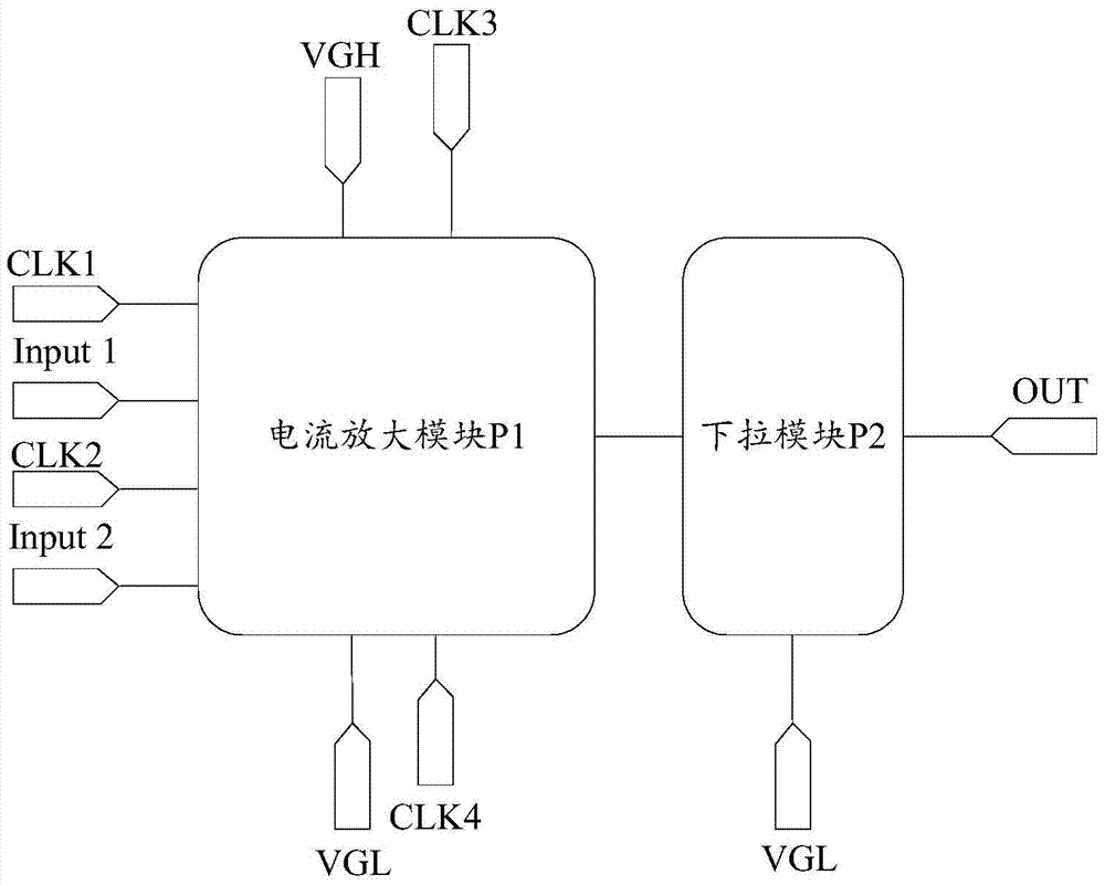
[0020] see figure 1 , the inverter provided by the embodiment of the present invention includes a current amplifying module P1 and a pull-down module P2; wherein, the current amplifying module P1 is connected to the first clock signal terminal CLK1, the second clock signal terminal CLK2, the third clock signal terminal CLK3, the fourth The clock signal terminal CLK4, the first input signal terminal Input1, the second input signal terminal Input 2, the high-level terminal VGH, the low-level terminal VGL, the pull-down module P2 and the output terminal OUT of the inverter, and the current amplification module P1 is used according to the first The signal of the first clock signal terminal CLK1, the signal of the second clock signal terminal CLK2, the signal of the third clock signal terminal CLK3, the signal of the fourth clock signal terminal CLK4, the signal of the first input signal terminal Input 1 and the second input signal terminal The signal of Input 2 amplifies the curre...
Embodiment 2
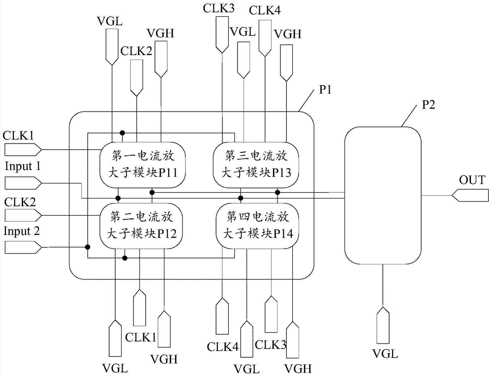
[0024] see figure 2 The current amplifying module P1 in the first embodiment may include a first current amplifying sub-module P11, a second current amplifying sub-module P12, a third current amplifying sub-module P13, and a fourth current amplifying sub-module P14. Among them, the first current amplification sub-module P11 is connected to the first clock signal terminal CLK1, the second clock signal terminal CLK2, the first input signal terminal Input1, the second input signal terminal Input 2, the high level terminal VGH, the low level terminal VGL, the first The second current amplifying sub-module P12, the third current amplifying sub-module P13, the fourth current amplifying sub-module, the pull-down module P2 and the output terminal OUT of the inverter, and the first current amplifying sub-module P11 is used for the first clock signal terminal CLK1 The signal of the second clock signal terminal CLK2, the signal of the first input signal terminal Input 1 and the signal o...
Embodiment 3
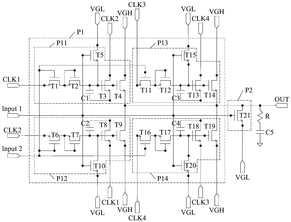
[0028] see image 3 , the first current amplifying sub-module P11, the second current amplifying sub-module P12, the third current amplifying sub-module P13, the fourth current amplifying sub-module P14 and the pull-down module P2 in the second embodiment will be described in detail below The specific composition structure, and the connection relationship between the specific composition structure of the first current amplification sub-module P11, the second current amplification sub-module P12, the third current amplification sub-module P13, the fourth current amplification sub-module P14 and the pull-down module P2 .
[0029] The first current amplifying sub-module P11 includes a first transistor T1, a second transistor T2, a third transistor T3, a fourth transistor T4, a fifth transistor T5 and a first capacitor C1; wherein, the gate of the first transistor T1 is connected to the second The input signal terminal Input 2, the second current amplifying sub-module P12, the th...
PUM
 Abstract
Description
Claims
Application Information
 - R&D
- Intellectual Property
- Life Sciences
- Materials
- Tech Scout
- Unparalleled Data Quality
- Higher Quality Content
- 60% Fewer Hallucinations
Browse by: Latest US Patents, China's latest patents, Technical Efficacy Thesaurus, Application Domain, Technology Topic, Popular Technical Reports.
© 2025 PatSnap. All rights reserved.Legal|Privacy policy|Modern Slavery Act Transparency Statement|Sitemap|About US| Contact US: help@patsnap.com